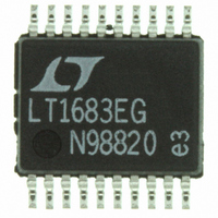
LTC1562CG#PBF Linear Technology, LTC1562CG#PBF Datasheet - Page 4

LTC1562CG#PBF
Manufacturer Part Number
LTC1562CG#PBF
Description
IC FILTER UNIV RC QUAD LN 20SSOP
Manufacturer
Linear Technology
Datasheet
1.LTC1562CGPBF.pdf
(28 pages)
Specifications of LTC1562CG#PBF
Filter Type
Universal, Continuous-Time
Frequency - Cutoff Or Center
150kHz
Number Of Filters
4
Max-order
8th
Voltage - Supply
4.75 V ~ 10.5 V, ±4.75 V ~ 5.25 V
Mounting Type
Surface Mount
Package / Case
20-SSOP
Lead Free Status / RoHS Status
Lead free / RoHS Compliant
Available stocks
Company
Part Number
Manufacturer
Quantity
Price
LTC1562
TYPICAL PERFOR A CE CHARACTERISTICS
PI FU CTIO S
Power Supply Pins: The V
bypassed with 0.1 F capacitors to an adequate analog
ground or ground plane. These capacitors should be
connected as closely as possible to the supply pins. In the
20-lead SSOP package, the additional pins 4, 7, 14 and 17
are internally connected to V
tied to the same point as Pin 16 for best shielding. Low
noise linear supplies are recommended. Switching sup-
plies are not recommended as they will lower the filter
dynamic range.
4
40
10
– 5
60
55
50
45
35
30
25
20
15
35
30
25
20
15
10
U
5
0
60
50
Q Error vs Nominal f
LP Noise vs Nominal f
(V
V2 Output) (R
R
S
IN
60
70
= 5V, 25 C) (Figure 3,
= R
U
70
Q
T
T
80
A
A
= 70 C
= 25 C
80
NOMINAL f
NOMINAL f
90
90
IN
Q = 2.5
Q = 5
Q = 1
100 110
= R2)
100
U
O
O
110
(kHz)
O
(kHz)
(V
O
120
S
120 130 140
W
= 2.5V)
130
–
+
(Pin 16) and should also be
Q = 2.5
Q = 10
Q = 1
Q = 5
140
1562 G07
and V
1562 G04
U
150
–
pins should be
– 0.5
3.0
2.5
2.0
1.5
1.0
0.5
40
60
55
50
45
35
30
25
20
15
10
0
50
60
Peak BP Gain vs Nominal f
(V
BP Noise vs Nominal f
(V
V1 Output) (R
R
S
S
IN
60
70
= 5V) (Figure 3, V1 Output)
= 5V, 25 C) (Figure 3,
= R
70
Q
T
T
80
A
A
= 70 C
= 25 C
80
NOMINAL f
NOMINAL f
90
90 100
IN
Q = 2.5
Q = 1
Q = 5
100 110
= R
Analog Ground (AGND): The AGND pin is the midpoint of
an internal resistive voltage divider, developing a potential
halfway between the V
series resistance nominally 7k . This serves as an inter-
nal ground reference. Filter performance will reflect the
quality of the analog signal ground and an analog ground
plane surrounding the package is recommended. The
analog ground plane should be connected to any digital
ground at a single point. For dual supply operation, the
AGND pin should be connected to the ground plane
O
O
110 120 130
Q
(kHz)
(kHz)
)
O
120 130 140
O
Q = 10
Q = 2.5
Q = 5
Q = 1
140
1562 G08
1562 G5
150
–100
– 0.5
–20
–30
– 40
– 50
– 60
– 80
–10
–70
– 90
1.5
1.0
3.0
2.5
2.0
0.5
+
0
0
and V
10k
50
Peak BP Gain vs Nominal f
(V
Distortion vs External Load
Resistance (V
(Figure 8)
2nd ORDER LOWPASS
f
Q = 0.7
OUTPUT LEVEL 1V
R
O
S
5V SUPPLIES
IN
60
= 100kHz
= 2.5V) (Figure 3, V1 Output)
= R
EXTERNAL LOAD RESISTANCE ( )
–
70
Q
T
T
pins, with an equivalent
A
A
= 70 C
= 25 C
80
NOMINAL f
5k
90 100
f
f
IN
IN
S
RMS
= 50kHz
= 20kHz
= 5V, 25 C)
(2.83V
O
110 120 130
(kHz)
Q = 10
2k
P-P
)
O
Q = 2.5
Q = 5
Q = 1
140
1562 G09
1562 G6
1562fa
150
1k


