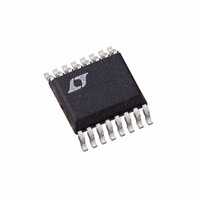
LTC1564IG#PBF Linear Technology, LTC1564IG#PBF Datasheet - Page 8

LTC1564IG#PBF
Manufacturer Part Number
LTC1564IG#PBF
Description
IC ANTIALIASING FILTER 16-SSOP
Manufacturer
Linear Technology
Datasheet
1.LTC1564CGPBF.pdf
(12 pages)
Specifications of LTC1564IG#PBF
Filter Type
Antialiasing
Frequency - Cutoff Or Center
150kHz
Number Of Filters
1
Max-order
8th
Voltage - Supply
2.7 V ~ 10.5 V
Mounting Type
Surface Mount
Package / Case
16-SSOP
Ic Filter Type
Lowpass
Filter Order
8th
No. Of Filters
1
Cutoff Frequency
150kHz
Supply Voltage Range
2.7V To 10.5V
Operating Temperature Range
-40°C To +85°C
Filter Ic Case Style
SSOP
Rohs Compliant
Yes
Lead Free Status / RoHS Status
Lead free / RoHS Compliant
Available stocks
Company
Part Number
Manufacturer
Quantity
Price
BLOCK DIAGRA
LTC1564
PI FU CTIO S
IN (Pin 16): Analog Input. The filter in the LTC1564 senses
the voltage difference between the IN and AGND pins. In
normal filtering (EN = 0, RST = 1, F code other than 0000),
the IN pin connects within the LTC1564 to a digitally
controlled resistance whose other end is a current-sum-
ming point at the AGND potential. At unity gain (G code
0000), the value of this input resistance is nominally 10k
and the IN voltage range is rail-to-rail (V
filtering at gain settings above unity (G code ≠ 0000), the
input resistance falls as (1/gain) to nominally 625Ω at a
gain of 16 (G code 1111) and the linear input range also
falls in inverse proportion to gain. (The variable gain
capability is designed to boost lower level input signals
with good noise performance.) Input resistance does not
vary significantly with the frequency-setting F code ex-
cept in the mute state (F code 0000). In either the mute
state (F code 0000 or RST = 0) or the shutdown state (EN
= 1 or EN open circuited), analog switches disconnect the
IN pin internally and this pin presents a very high input
8
U
U
V
V
EN
IN
+
–
U
W
V
V
+
–
SHUTDOWN
SWITCH
SHUTDOWN
SWITCH
R
R
AGND
+
to V
–
Figure 3. Block Diagram
). When
G3
AMPLIFIER
VARIABLE
G2
GAIN
G1
resistance. Circuitry driving the IN pin must be compat-
ible with the LT1564’s input resistance and with the
variation of this resistance in the event that the LTC1564
is used in multiple modes. Signal sources with significant
output resistance may introduce a gain error as the
source’s output resistance and the LTC1564’s input resis-
tance form a voltage divider. This is especially true at the
higher gain or G code settings where the LTC1564’s input
resistance is lowest.
In single supply voltage applications with elevated gain
settings (G code ≠ 0000) it is important to keep in mind
that the LTC1564’s ground reference point is AGND, not
V
voltage range is no longer rail-to-rail but converges
toward AGND. Similarly the OUT pin swings positive or
negative with respect to AGND. At unity gain (G code
0000), both IN and OUT voltages can swing from rail-to-
rail.
–
G0
CMOS LATCH
. With increasing gains, the LTC1564’s linear input
PROGRAMMABLE FILTER
F3
F2
F1
F0
1564 F03
OUT
CS/HOLD
RST
1564fa


