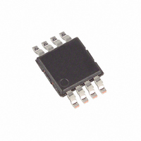
MAX7427EUA+ Maxim Integrated Products, MAX7427EUA+ Datasheet - Page 10

MAX7427EUA+
Manufacturer Part Number
MAX7427EUA+
Description
IC FILTER LOWPASS 5TH 8UMAX
Manufacturer
Maxim Integrated Products
Datasheet
1.MAX7427CUA.pdf
(12 pages)
Specifications of MAX7427EUA+
Filter Type
Elliptic, Lowpass Switched Capacitor
Frequency - Cutoff Or Center
12kHz
Number Of Filters
1
Max-order
5th
Voltage - Supply
2.7 V ~ 3.6 V
Mounting Type
Surface Mount
Package / Case
8-MSOP, Micro8™, 8-uMAX, 8-uSOP,
Number Of Channels
Single
Cutoff Frequency
12 KHz
Supply Voltage (max)
3 V
Maximum Operating Temperature
+ 85 C
Minimum Operating Temperature
- 40 C
Mounting Style
SMD/SMT
Operating Supply Voltage
3 V
Supply Voltage (min)
2.7 V
Lead Free Status / RoHS Status
Lead free / RoHS Compliant
5th-Order, Lowpass, Elliptic,
Switched-Capacitor Filters
Figure 4. Dual-Supply Operation
Characteristics table for the input voltage range of COM
and OS. Changing the voltage on COM or OS signifi-
cantly from midsupply reduces the dynamic range.
The MAX7426 operates from a single +5V supply, and
the MAX7427 operates from a single +3V supply.
Bypass V
supplies are required, connect COM to the system
ground and GND to the negative supply. Figure 4
shows an example of dual-supply operation. Single-
supply and dual-supply performance are equivalent.
Table 2. Typical Harmonic Distortion
10
V+
V-
*CONNECT SHDN TO V- FOR LOW-POWER SHUTDOWN MODE.
MAX7426
MAX7427
______________________________________________________________________________________
FILTER
DD
CLOCK
INPUT
to GND with a 0.1µF capacitor. If dual
IN
CLK
(kHz)
f
500
100
500
100
CLK
MAX7426
MAX7427
V
GND
V+
DD
V-
SHDN
COM
OUT
OS
Power Supplies
*
0.1µF
OUTPUT
(Hz)
200
200
f
1k
1k
IN
0.1µF
(Vp-p)
V
4
2
For either single-supply or dual-supply operation, drive
CLK and SHDN from GND (V- in dual-supply operation)
to V
MAX7426 for ±1.5V. For ±5V dual-supply applications,
refer to the MAX291/MAX292/MAX295/MAX296 and
MAX293/MAX294/MAX297 data sheets.
The optimal input signal range is determined by observ-
ing the voltage level at which the signal-to-noise plus
distortion (SINAD) ratio is maximized for a given corner
frequency. The Typical Operating Characteristics show
the THD + Noise response as the input signal’s peak-to-
peak amplitude is varied.
When using the MAX7426/MAX7427 for anti-aliasing or
post-DAC filtering, synchronize the DAC (or ADC) and
the filter clocks. If the clocks are not synchronized,
beat frequencies may alias into the desired passband.
Harmonic distortion arises from nonlinearities within the
filter. These nonlinearities generate harmonics when a
pure sine wave is applied to the filter input. Table 2 lists
typical harmonic distortion values with a 10kΩ load at
T
TRANSISTOR COUNT: 1457
PROCESS: BiCMOS
IN
A
= +25°C.
DD
. Use the MAX7427 for ±2.5, and use the
Anti-Aliasing and Post-DAC Filtering
2nd
-71
-88
-87
-90
TYPICAL HARMONIC DISTORTION (dB)
Input Signal Amplitude Range
3rd
-73
-86
-86
-87
Chip Information
Harmonic Distortion
4th
-90
-92
-90
-90
5th
-82
-88
-90
-90


