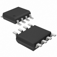
MAX7480ESA+ Maxim Integrated Products, MAX7480ESA+ Datasheet - Page 7

MAX7480ESA+
Manufacturer Part Number
MAX7480ESA+
Description
IC FILTER LOWPASS 8TH 8-SOIC
Manufacturer
Maxim Integrated Products
Datasheet
1.MAX7480ESA.pdf
(8 pages)
Specifications of MAX7480ESA+
Filter Type
Butterworth, Lowpass Switched Capacitor
Frequency - Cutoff Or Center
2kHz
Number Of Filters
4
Max-order
8th
Voltage - Supply
4.5 V ~ 5.5 V
Mounting Type
Surface Mount
Package / Case
8-SOIC (3.9mm Width)
Number Of Channels
Single
Cutoff Frequency
2 KHz
Supply Voltage (max)
5 V
Maximum Operating Temperature
+ 85 C
Minimum Operating Temperature
- 40 C
Mounting Style
SMD/SMT
Supply Voltage (min)
4.5 V
Lead Free Status / RoHS Status
Lead free / RoHS Compliant
The MAX7480 SCF is designed for use with external
clocks that have a 40% to 60% duty cycle. When using
an external clock with these devices, drive CLK with a
CMOS gate powered from 0 to V
the external clock adjusts the corner frequency of the
filter as follows:
When using the internal oscillator, connect a capacitor
(C
capacitor determines the oscillator frequency as follows:
Minimize the stray capacitance at CLK so that it does
not affect the internal oscillator frequency. Vary the rate
of the internal oscillator to adjust the filter’s corner fre-
quency by a 100:1 clock to corner-frequency ratio. For
example, an internal oscillator frequency of 100kHz
produces a nominal corner frequency of 1kHz.
The MAX7480’s input impedance is effectively that of a
switched-capacitor resistor, and is inversely proportion-
al to frequency. The input impedance values deter-
mined below represent the average input impedance,
since the input current is not continuous. As a rule, use
a driver with an output impedance less than 10% of the
filter’s input impedance. Estimate the input impedance
of the filter using the following formula:
where f
This device features a shutdown mode that is activated
by driving SHDN low. In shutdown mode, the filter’s sup-
ply current reduces to 0.2µA (typ) and its output
becomes high impedance. For normal operation, drive
SHDN high or connect to V
The voltage at COM sets the common-mode input volt-
age and is biased at mid-supply with an internal resis-
tor-divider. Bypass COM with a 0.1µF capacitor and
___________Applications Information
OSC
Input Impedance vs. Clock Frequencies
) between CLK and ground. The value of the
CLK
f
OSC
= clock frequency and C
(kHz)
Z
_______________________________________________________________________________________
IN
Low-Power Shutdown Mode
f
C
Offset and Common-Mode
= f
53 10
C
f
CLK
CLK
DD
OSC
.
3
/ 100
1
; C
C
DD
Input Adjustment
IN
OSC
8th-Order, Lowpass, Butterworth,
. Varying the rate of
IN
= 2.31pF.
in pF
Clock Signal
External Clock
Internal Clock
Switched-Capacitor Filter
connect OS to COM. For applications requiring offset
adjustment or DC level shifting, apply an external bias
voltage through a resistor-divider network to OS, as
shown in Figure 3. (Note: Do not leave OS unconnect-
ed.) The output voltage is represented by this equation:
with V
lowpass-filtered by the SCF and VOS is added at the
output stage. See the Electrical Characteristics for the
voltage range of COM and OS. Changing the voltage
on COM or OS significantly from mid-supply reduces
the filter’s dynamic range.
The MAX7480 operates from a single +5V supply.
Bypass V
supplies (±2.5V) are required, connect COM to system
ground and connect GND to the negative supply.
Figure 4 shows an example of dual-supply operation.
Single- and dual-supply performances are equivalent.
For either single- or dual-supply operation, drive CLK
and SHDN from GND (V- in dual-supply operation) to
V
MAX291–MAX297.
The optimal input signal range is determined by observ-
ing the voltage level at which the total harmonic distor-
tion plus noise (THD+N) is minimized for a given corner
frequency. The Typical Operating Characteristics
shows a graph of the device’s THD+N response as the
input signal’s peak-to-peak amplitude is varied. This
measurement is made with OS and COM biased at mid-
supply.
Figure 3. Offset Adjustment Circuit
DD
. For ±5V dual-supply applications, use the
0.1 F
COM
CLOCK
INPUT
V
SUPPLY
DD
= V
to GND with a 0.1µF capacitor. If dual
V
DD
OUT
IN
CLK
Input Signal Amplitude Range
/ 2 (typical), where (V
= (V
MAX7480
V
GND
IN
DD
- V
COM
SHDN
COM
OUT
OS
) + V
Power Supplies
0.1 F
0.1 F
OS
OUTPUT
IN
- V
COM
50k
50k
50k
) is
7


