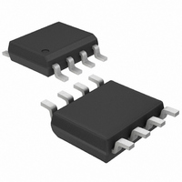
MAX295CSA+ Maxim Integrated Products, MAX295CSA+ Datasheet - Page 7

MAX295CSA+
Manufacturer Part Number
MAX295CSA+
Description
IC FILTER LOWPASS 8-SOIC
Manufacturer
Maxim Integrated Products
Datasheet
1.MAX291CSA.pdf
(10 pages)
Specifications of MAX295CSA+
Filter Type
Butterworth, Lowpass Switched Capacitor
Frequency - Cutoff Or Center
25kHz
Number Of Filters
1
Max-order
8th
Voltage - Supply
4.75 V ~ 11 V, ±2.375 V ~ 5.5 V
Mounting Type
Surface Mount
Package / Case
8-SOIC (3.9mm Width)
Number Of Channels
Single
Cutoff Frequency
50 KHz
Supply Voltage (max)
11 V
Maximum Operating Temperature
+ 70 C
Minimum Operating Temperature
0 C
Mounting Style
SMD/SMT
Supply Voltage (min)
4.75 V
Lead Free Status / RoHS Status
Lead free / RoHS Compliant
error on its respective poles, while the same mismatch in a
ladder filter design will spread its error over all poles.
The MAX291/MAX292/MAX295/MAX296 input impedance
is effectively that of a switched-capacitor resistor (see
equation below, and Table 1), and it is inversely proportion-
al to frequency. The input impedance values determined
below represent average input impedance, since the input
current is not continuous. The input current flows in a series
of pulses that charge the input capacitor every time the
appropriate switch is closed. A good rule of thumb is that
the driver’s input source resistance should be less than
10% of the filter’s input impedance. The input impedance
of the filter can be estimated using the following formula:
where: f
The input impedance for various clock frequencies is
given below:
The MAX291/MAX292/MAX295/MAX296 maximum rec-
ommended clock frequency is 2.5MHz, producing a cutoff
frequency of 25kHz for the MAX291/MAX292 and 50kHz
for the MAX295/MAX296. The CLK pin can be driven by
an external clock or by the internal oscillator with an exter-
nal capacitor. For external clock applications, the clock
circuitry has been designed to interface with +5V CMOS
logic. Drive the CLK pin with a CMOS gate powered from
0V and +5V when using either a single +5V supply or dual
+5V supplies. The MAX291/MAX292/MAX295/MAX296
supply current increases slightly (<3%) with increasing
Figure 2. 8th-Order Ladder Filter Network
Table 1. Input Impedance for Various Clock
Frequencies
MAX291
MAX292
MAX295
MAX296
V
PART
IN
R1
CLK
= Clock Frequency
L1
C (pF)
3.28
4.47
4.22
2.24
C2
Z = 1 / (f
_______________________________________________________________________________________
Clock-Signal Requirements
L3
C4
10kHz
(MΩ)
44.6
30.5
22.4
23.7
CLK
* C)
L5
C6
100kHz
(MΩ)
4.46
3.05
2.24
2.37
L7
C8
1000kHz
(kΩ)
446
305
224
237
Switched-Capacitor Filters
R2
V
O
clock frequency over the clock range 100kHz to 1MHz.
Varying the rate of an external clock will dynamically ad-
just the corner frequency of the filter.
Ideally, the MAX291/MAX292/MAX295/MAX296 should
be clocked symmetrically (50% duty cycle). MAX291/
MAX292/MAX295/MAX296 can be operated with clock
asymmetry of up to 60/40% (or 40/60%) if the clock
remains HIGH and LOW for at least 200ns. For example,
if the part has a maximum clock rate of 2.5MHz, then the
clock should be high for at least 200ns, and low for at
least 200ns.
When using the internal oscillator, the capacitance (C
from CLK to ground determines the oscillator frequency:
The stray capacitance at CLK should be minimized be-
cause it will affect the internal oscillator frequency.
The MAX291/MAX292/MAX295/MAX296 operate from
either dual or single power supplies. The dual-supply volt-
age range is +2.375V to +5.500V. The ±2.5V dual supply is
equivalent to single-supply operation (Figure 3). Minor per-
formance degradation could occur due to the external
resistor divider network, where the GND pin is biased to
mid-supply.
The ideal input signal range is determined by observing at
what voltage level the total harmonic distortion plus noise
(THD + Noise) ratio is maximized for a given corner fre-
quency. The Typical Operating Characteristics show the
MAX291/MAX292/MAX295/MAX296 THD + Noise response
as the input signal’s peak-to-peak amplitude is varied.
The uncommitted op amp has its noninverting input tied
to the GND pin, and can be used to build a 1st- or 2nd-
Figure 3. +5V Single-Supply Operation
___________Application Information
Pin Configuration is 8-pin DIP.
+5V
INPUT SIGNAL
0V
+1V TO +4V
RANGE
8th-Order, Lowpass,
1
3
4
8
f
OSC
CLK
OP OUT
OP IN-
IN
MAX29_
(
kHz
2
7
V-
V+
)
GND
≈
OUT
Uncommitted Op Amp
3
C
5
6
Input Signal Range
0.1µF
OSC
10
5
Power Supplies
(
pF
)
10k
10k
+5V
OUTPUT
0.1µF
0V
OSC
7
)


