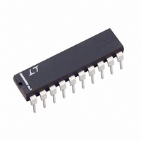
LTC1060CN Linear Technology, LTC1060CN Datasheet - Page 18

LTC1060CN
Manufacturer Part Number
LTC1060CN
Description
IC FILTER BUILDING BLOCK 20-DIP
Manufacturer
Linear Technology
Datasheet
1.LTC1060CNPBF.pdf
(20 pages)
Specifications of LTC1060CN
Filter Type
Universal Switched Capacitor
Frequency - Cutoff Or Center
30kHz
Number Of Filters
2
Max-order
4th
Voltage - Supply
±2.37 V ~ 5 V
Mounting Type
Through Hole
Package / Case
20-DIP (0.300", 7.62mm)
Lead Free Status / RoHS Status
Contains lead / RoHS non-compliant
Available stocks
Company
Part Number
Manufacturer
Quantity
Price
COMM
Switched capacitor integrators generally exhibit higher
input offsets than discrete R, C integrators. These offsets
are mainly due to the charge injection of the CMOS
switches into the integrating capacitors and they are
temperature independent.
The internal op amp offsets also add to the overall offset
budget and they are typically a couple of millivolts. Be-
cause of this, the DC output offsets of switched capacitor
filters are usually higher than the offsets of discrete active
filters.
LTC1060
LTC1060 OFFSETS
18
Figure 22. Combining Mode 3 with Mode 2b to Create a 4th
Order BR Elliptic Filter with 1dB Ripple and a Ratio of 0dB to
Stop Bandwidth Equal to 9/1.
Figure 24. Equivalent Input Offsets of 1/2 LTC1060 Filter
Building Block
(17)
V
4
IN
+
W W
V
R11
OS1
15
T
–
2
L OR CMOS
–
+
CLOCK IN
V
R11 = 60k
R41 = 28.84k
R52 = 5k
R32 = 455.75k
R41
R31
R21
E TS
+
= –5V
U
–5V
(18) (16)
3
+
10
1
2
3
4
5
6
7
8
9
ON
5
RESISTOR VALUES
LP
BP
HP
INV
S1A
S
V
V
LSh
CLK
R21 = 5k
R
R62 = 1.59k
R42 = 503.85k
–
–
A/B
A
D
H1
A
+
+
A
A
+
U
A
LTC1060
A
= 5k
V
OS2
R
R
H1
L1
–
THE
50/100
AGND
CLK
INV
–
+
LP
BP
S1B
V
V
N
D
A
B
B
B
B
B
–
–
20
19
18
17
16
15
14
13
12
11
R31 = 54.75k
R
R22 = 60k
L1
M
W
= 19.3k
R42
R52
R32
R22
V
(19)
–
2
ODES OF OPERATIO
= –5V
+
V
OS3
–
–
+
R62
LTC1060 • CM04
TLC1060 • LO01
V
OUT
(20)
1
Figure 24 shows half of an LTC1060 filter building block
with its equivalent input offsets V
are 100% tested for both sides of the LTC1060. V
generally the larger offset. When the S
LTC1060 is shorted to the negative supply (i.e., mode 3),
the value of the V
low, a 20% to 30% noise reduction is observed. Mode 1
can still be achieved, if desired, by shorting the S1 pin to
the lowpass output (Figure 25).
Figure 23. Amplitude Response of the Notch Filter of Figure 22
Figure 25. Mode 1(LN): Same Operation as Mode 1 but Lower
V
OS2
Offset and Lower Noise
– 40
– 50
– 60
–10
–20
–30
V
IN
0
0.7
S
R1
V
A/B
INPUT FREQUENCY NORMALIZED TO FILTER CENTER FREQUENCY
6
U
f
CLK
–
f
0
(17)
15
=
4
200
1
0.8
OS2
–
+
; f
CLK
R3
R2
decreases. Additionally, with S
≤ 1MHz
0.9
3
f
N
(18)
0
1/2 LTC1060
= 1.0
+ –
5
OS1
–
S1A
(16)
, V
1.1
OS2
A/B
2
TLC1060 • LO02
BP
(19)
, V
, Pin 6, of the
1.2
OS3
1
TLC1060 • CMO05
LP
(20)
. All three
OS2
1.3
1060fb
A/B
is


