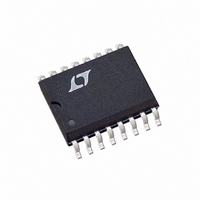
LTC1065CSW Linear Technology, LTC1065CSW Datasheet - Page 4

LTC1065CSW
Manufacturer Part Number
LTC1065CSW
Description
IC FILTR 5TH ORDR LOWPASS 16SOIC
Manufacturer
Linear Technology
Datasheet
1.LTC1065CSWPBF.pdf
(16 pages)
Specifications of LTC1065CSW
Filter Type
Bessel, Lowpass Switched Capacitor
Frequency - Cutoff Or Center
50kHz
Number Of Filters
1
Max-order
5th
Voltage - Supply
±2.375 V ~ 8 V
Mounting Type
Surface Mount
Package / Case
16-SOIC (0.300", 7.5mm Width)
Lead Free Status / RoHS Status
Contains lead / RoHS non-compliant
Other names
LTC1065CS
Available stocks
Company
Part Number
Manufacturer
Quantity
Price
Part Number:
LTC1065CSW
Manufacturer:
LTNEAR
Quantity:
20 000
Company:
Part Number:
LTC1065CSW#PBF
Manufacturer:
LTC
Quantity:
206
Note 1: Absolute Maximum Ratings are those values beyond which the life
of a device may be impaired.
Note 2: The maximum clock frequency is arbitrarily defined as the
frequency at which the filter AC response exhibits ≥ 1dB of gain peaking.
Note 3: At limited temperature ranges (i.e., T
frequency can be as low as 10Hz. The typical minimum clock frequency is
arbitrarily defined as the clock frequency at which the output DC offset
changes by more than 1mV.
Note 4: The wideband noise specification does not include the clock
feedthrough.
ELECTRICAL C
TYPICAL PERFOR
LTC1065
4
–20
–30
–40
–50
–60
–70
–80
–90
–10
110
100
10
90
80
70
60
50
40
30
20
10
0
1
Self-Clocking Frequency vs R
Gain vs Frequency; V
A. f
B. f
C. f
V
T
100
IN
A
= 25°C
CLK
CLK
CLK
= 750mV
= 0.5MHz
= 1MHz
= 2MHz
INPUT FREQUENCY (kHz)
FREQUENCY (kHz)
RMS
10
300
A
C = 200pF
f
OSC
4
HARA TERISTICS
S
B
LTC1065
≅ 1/RC
= ±2.5V
R
C
W
5
100
500
A
1065 G04
C
1065 G01
C
U
200
A
≤ 50°C) the minimum clock
CE
C
–10
–20
–30
–40
–50
–60
–70
–80
–90
HARA TERISTICS
10
50
45
40
35
30
25
20
15
10
0
5
0
10
Gain vs Frequency; V
1
Output Offset vs Clock,
Low Clock Rates
A
A. f
B. f
C. f
D. f
V
T
V
A. T
B. T
IN
A
S
= 25°C
CLK
CLK
CLK
CLK
EXTERNAL CLOCK FREQUENCY (Hz)
= ±5V
= 1.4V
A
A
B
= 25°C
= 85°C
= 1MHz
= 2MHz
= 3MHz
= 4MHz
C
INPUT FREQUENCY (kHz)
RMS
10
110
Note 5: To properly evaluate the filter’s harmonic distortion an inverting
output buffer is recommended. An output buffer (although recommended)
is not necessarily needed when measuring output DC offset or wideband
noise (see Figure 3).
Note 6: The output DC offset is optimized for ±5V supply. The output DC
offset shifts when the power supplies change; however, this phenomenon
is repeatable and predictable.
Note 7: The LTC1065C is guaranteed to meet the specified performance
from 0°C to 70°C and is designed, characterized and expected to meet
specified performance from –40°C to 85°C but is not tested or QA
sampled at these temperatures. The LTC1065I is guaranteed to meet
specified performance from –40°C to 85°C.
S
A
= ±5V
B C
100
1065 G05
1065 G02
D
200
210
–10
–20
–30
–40
–50
–60
–70
–80
–90
–1
–2
–3
–4
–5
10
0
5
4
3
2
1
0
0
1
Output Offset vs Clock,
Medium Clock Rates
Gain vs Frequency; V
A. f
B. f
C. f
D. f
E. f
V
T
A
IN
V
V
V
EXTERNAL CLOCK FREQUENCY (kHz)
= 25°C
CLK
CLK
CLK
CLK
CLK
S
S
S
= 1.4V
= ±7.5V
= ±5V
= ±2.5V
= 5MHz
= 1MHz
= 2MHz
= 3MHz
= 4MHz
INPUT FREQUENCY (kHz)
RMS
10
500
A
S
B C
= ±7.5V
100
1065 G06
1065 G03
D
E
1065fb
1000
200


