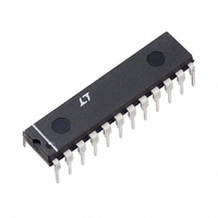
LTC1064CN Linear Technology, LTC1064CN Datasheet - Page 10

LTC1064CN
Manufacturer Part Number
LTC1064CN
Description
IC FILTER BUILDNG BLK QUAD 24DIP
Manufacturer
Linear Technology
Datasheet
1.LTC1064CNPBF.pdf
(20 pages)
Specifications of LTC1064CN
Filter Type
Universal Switched Capacitor
Frequency - Cutoff Or Center
140kHz
Number Of Filters
4
Max-order
8th
Voltage - Supply
±2.375 V ~ 8 V
Mounting Type
Through Hole
Package / Case
24-DIP (0.300", 7.62mm)
Lead Free Status / RoHS Status
Contains lead / RoHS non-compliant
Available stocks
Company
Part Number
Manufacturer
Quantity
Price
Part Number:
LTC1064CN
Manufacturer:
LT
Quantity:
20 000
W
LTC1064
V
10
Mode 3a
This is an extension of Mode 3 where the highpass and
lowpass outputs are summed through two external resis-
tors R
Mode 3a is more versatile than Mode 2 because the notch
frequency can be higher or lower than the center fre-
quency of the 2nd order section. The external op amp of
Figure 9 is not always required. When cascading the
sections of the LTC1064, the highpass and lowpass
V
IN
IN
ODES OF OPERATIO
R1
R1
H
and R
AGND
AGND
–
+
L
R4
R3
R2
to create a notch. This is shown in Figure 9.
–
+
R4
R3
R2
Figure 9. Mode 3a: 2nd Order Filter Providing Highpass, Bandpass, Lowpass and Notch
HP
+
C
C
Figure 8. Mode 2: 2nd Order Filter Providing Notch, Bandpass and Lowpass
Σ
–
S
N
1/4 LTC1064
+
1/4 LTC1064
∫
Σ
R
–
H
S
U
BP
∫
∫
LP
BP
R
L
∫
EXTERNAL OP AMP OR INPUT
OP AMP OF THE LTC1064,
SIDE A, B, C, D
+
1064 F08
–
R
LP
G
R3 =
MODE 2 (100:1):
MODE 2 (50:1):
NOTE: THE 50:1 EQUATIONS FOR MODE 2 ARE DIFFERENT FROM THE EQUATIONS
FOR MODE 2 OPERATION OF THE LTC1059, LTC1060 AND LTC1061. START WITH
f
O
, CALCULATE R2/R4, SET R4; FROM THE Q VALUE, CALCULATE R3:
MODE 3a (100:1):
MODE 3a (50:1):
outputs can be summed directly into the inverting input of
the next section. The topology of Mode 3a is useful for
elliptic highpass and notch filters with clock-to-cutoff
frequency ratios higher than 100:1. This is often required
to extend the allowed input signal frequency range and to
avoid premature aliasing.
When the internal clock-to-center frequency ratio is set at
50:1, the design equations for Q and bandpass gain are
different from the 100:1 case .
1.005
NOTCH
Q
1064 F09
√
R2
1 +
R2
R4
f
H
f
H
O
O
OBP
OBP
+
H
H
f
H
f
NOTE: THE 50:1 EQUATIONS FOR MODE 3A ARE DIFFERENT FROM
THE EQUATIONS FOR MODE 3A OPERATION OF THE LTC1059,
LTC1060 AND LTC1061. START WITH f
FROM THE Q VALUE, CALCULATE R3:
=
=
R3 =
O
O
16R4
OLP
OBP
ON
f
f
100
R2
=
=
CLK
CLK
50
= –
= –
(f = f
f
100
f
CLK
CLK
50
= –
1.005
= –
√
1 –
√
Q
R3
R1
; THEN CALCULATE R1 TO SET THE DESIRED GAIN.
O
1 +
√
√
) = Q
1 –
1 +
R4
R1
R3
R1
; H
16R4
1 +
R3
√
R2
R4
R2
R3
R1
; H
R2
R4
16R4
ON1
R2
R4
R3
R2
R4
(
; f
R2
R4
ON1
; H
R
R
; f
(f→ 0) = –
n
; f
G
L
+
n
=
(f→ 0) =
; f
; H
ON1
H
n
16R4
=
f
OLP
n
100
R2
=
CLK
OLP
f
=
CLK
50
(f→ 0) = –
f
CLK
f
50
–
CLK
50
(f = 0) =
√
; THEN CALCULATE R1 TO
; Q =
SET THE DESIRED GAIN.
( )( )
R
R
1 +
R
R
R
R
; Q =
G
H
√
H
L
G
R2
R1
L
H
1.005
; H
R2
R4
R
R
OHP
R4
R1
H
–
L
1 +
R3
R2
R2
R3
OHP
R4
R1
; H
; H
R2
R1
)
; H
; Q =
√
R2
R4
O
√
–
OHP
=
ON2
;
, CALCULATE R2/R4, SET R4;
Q =
ON2
1 +
16R4
–
1 +
R2
; H
R2
R1
(
(
f→
R3
R2
(
f→
R2
R4
ON2
R2
R4
f→
1.005
; HOBP =
R2
R3
√
f
f
CLK
CLK
; H
= f→
f
2
; H
2
CLK
–
R2
R4
=
= –
2
(
OLP
√
=
16R4
OLP
)
)
R2
)
R2
R4
–
= –
f
–
= –
CLK
2
R3
R1
( )( )
R2
R1
R2
R1
=
R
R
1 +
G
H
1 +
)
;
;
;
R2
R1
1064 F08Eq
1064 F09Eq
R2
R1
1064fb
R2
R1
R2
R4
–
R2
R4
R2
R1
;
;


