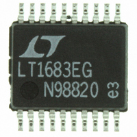
LTC1562CG Linear Technology, LTC1562CG Datasheet - Page 9

LTC1562CG
Manufacturer Part Number
LTC1562CG
Description
IC FILTER UNIVRSL RC QUAD 20SSOP
Manufacturer
Linear Technology
Datasheet
1.LTC1562CGPBF.pdf
(28 pages)
Specifications of LTC1562CG
Filter Type
Universal, Continuous-Time
Frequency - Cutoff Or Center
150kHz
Number Of Filters
4
Max-order
8th
Voltage - Supply
4.75 V ~ 10.5 V, ±4.75 V ~ 5.25 V
Mounting Type
Surface Mount
Package / Case
20-SSOP
Order Filter (max)
8th
Dual Supply Voltage (typ)
±3/±5V
Power Supply Requirement
Single/Dual
Single Supply Voltage (min)
4.75V
Dual Supply Voltage (min)
±2.375V
Operating Temperature (min)
0C
Operating Temperature (max)
70C
Operating Temperature Classification
Commercial
Lead Free Status / RoHS Status
Contains lead / RoHS non-compliant
Available stocks
Company
Part Number
Manufacturer
Quantity
Price
Company:
Part Number:
LTC1562CG#PBF
Manufacturer:
LTC
Quantity:
462
Company:
Part Number:
LTC1562CG#TRPBF
Manufacturer:
LINEAR
Quantity:
6 457
Part Number:
LTC1562CG#TRPBF
Manufacturer:
LINEAR/凌特
Quantity:
20 000
Part Number:
LTC1562CG-2
Manufacturer:
LINEAR/凌特
Quantity:
20 000
Company:
Part Number:
LTC1562CG-2#PBF
Manufacturer:
Linear Technology
Quantity:
135
Company:
Part Number:
LTC1562CG-2#PBF
Manufacturer:
LTC
Quantity:
200
Part Number:
LTC1562CG-2#PBF
Manufacturer:
LT凌特厂
Quantity:
20 000
Part Number:
LTC1562CG-2#TRPBF
Manufacturer:
LT凌特厂
Quantity:
20 000
APPLICATIONS
at frequency f
a frequency below f
Basic Bandpass
There are two different ways to obtain a bandpass function
in Figure 3, both of which give the following transfer
function form:
ously in Setting f
R
6a) with a gain parameter H
capacitor of value C
output (Figure 6b), with the same H
the gain parameter now H
transfer function has a gain magnitude of H
when the frequency equals f
at that frequency. Q measures the sharpness of the peak
(the ratio of f
pass function, as illustrated in Figure 4.
Basic Highpass
When Z
response appears at the V1 output (Figure 7).
V
IN
O
IN
H
, a bandpass response results at the V1 output (Figure
V s
= 2 f
V s
BP
IN
1
R
( )
( )
( )
IN
IN
s
(a) Resistive Input
O
INV
of Figure 3 is a capacitor of value C
and Q are set by R2 and R
Figure 6. Basic Bandpass Configurations
1/4 LTC1562
2nd ORDER
H
s
O
O
2
HP
V1
, and for Q > 0.707, a gain peak occurs at
to – 3dB bandwidth) in a 2nd order band-
–
( )
R
O
s
Q
H
and Q. When Z
IN
U
B
V2
O
O
, as shown in Figure 4.
gives a bandpass response at the V2
R2
/
s
Q s
2
O
V
INFORMATION
B
OUT
/
U
Q s
= (R
O
and has a phase shift of 180
B
–
O
V
Q
= R
O
H s
2
IN
/
/10k )(C
H
Q s
IN
Q
BP
W
2
C
Q
/R
is a resistor of value
IN
(b) Capacitive Input
(s) expression, and
as described previ-
IN
INV
. Alternatively, a
B
1/4 LTC1562
2nd ORDER
O
2
IN
(its peak value)
IN
/159pF). This
V1
, a highpass
R
U
Q
V2
R2
1562 F06
V
OUT
Parameters
above. The highpass gain parameter is H
For a 2nd order highpass response the gain magnitude at
frequency f
cies (f >> f
frequency above f
function includes a sign inversion.
Signal Swings
The V1 and V2 outputs are capable of swinging to within
roughly 100mV of each power supply rail. As with any
analog filter, the signal swings in each 2nd order section
must be scaled so that no output overloads (saturates),
even if it is not used as a signal output. (Filter literature
often calls this the “dynamics” issue.) When an unused
output has a larger swing than the output of interest, the
section’s gain or input amplitude must be scaled down to
avoid overdriving the unused output. The LTC1562 can
still be used with high performance in such situations as
long as this constraint is followed.
For an LTC1562 section as in Figure 3, the magnitudes of
the two outputs V2 and V1, at a frequency
the ratio,
regardless of the details of Z
quency above or below 100kHz produces larger output
amplitude at V1 or V2, respectively. This relationship can
guide the choice of filter design for maximum dynamic
range in situations (such as bandpass responses) where
there is more than one way to achieve the desired fre-
quency response with an LTC1562 section.
|
| ( ) |
V j
V j
2
1
( ) |
O
Figure 7. Basic Highpass Configuration
O
is QH
). For Q > 0.707, a gain peak occurs at a
V
O
IN
(
100
= 2 f
H
O
C
IN
, and approaches H
f
kHz
as shown in Figure 4. The transfer
O
INV
)
and Q are set by R2 and R
1/4 LTC1562
2nd ORDER
V1
R
IN
Q
. Therefore, an input fre-
V2
R2
1562 F07
V
H
OUT
at high frequen-
LTC1562
H
= C
= 2 f, have
IN
/159pF.
Q
1562fa
9
as


