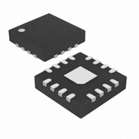
MAX7315ATE+ Maxim Integrated Products, MAX7315ATE+ Datasheet - Page 12

MAX7315ATE+
Manufacturer Part Number
MAX7315ATE+
Description
IC I/O EXPANDER I2C 8B 16TQFN-EP
Manufacturer
Maxim Integrated Products
Datasheet
1.MAX7315ATE.pdf
(26 pages)
Specifications of MAX7315ATE+
Interface
I²C, SMBus
Number Of I /o
8
Interrupt Output
Yes
Frequency - Clock
400kHz
Voltage - Supply
2 V ~ 3.6 V
Operating Temperature
-40°C ~ 125°C
Mounting Type
Surface Mount
Package / Case
16-TQFN Exposed Pad
Operating Supply Voltage
2 V to 3.6 V
Power Dissipation
1176 mW
Operating Temperature Range
- 40 C to + 125 C
Input Voltage
1.08 V to 1.4 V
Maximum Clock Frequency
400 KHz
Mounting Style
SMD/SMT
Output Voltage
0.15 V
Chip Configuration
8 Bit
Bus Frequency
400kHz
Ic Interface Type
I2C, SMBus
No. Of I/o's
8
Supply Voltage Range
2V To 3.6V
Digital Ic Case Style
TQFN
No. Of Pins
16
Filter Terminals
SMD
Rohs Compliant
Yes
Lead Free Status / RoHS Status
Lead free / RoHS Compliant
8-Port I/O Expander with LED Intensity
Control, Interrupt, and Hot-Insertion Protection
The command address stored in the MAX7315 circu-
lates around grouped register functions after each data
byte is written or read (Table 2).
If a device reset input is needed, consider the
MAX7316. The MAX7316 includes a RST input, which
clears any transaction to or from the MAX7316 on the
serial interface and configures the internal registers to
the same state as a power-up reset.
Figure 10. Read, Write, and Interrupt Timing Diagrams
12
P7–P0
P7–P0
P7–P0
SCL
SDA
WRITE TO OUTPUT PORTS REGISTERS (BLINK PHASE 0 REGISTERS/BLINK PHASE 1 REGISTERS)
READ FROM INPUT PORTS REGISTERS
INTERRUPT VALID/RESET
SCL
SDA
SCL
SDA
______________________________________________________________________________________
INT
Command Address Autoincrementing
S A6 A5 A4 A3 A2 A1 A0
S A6 A5 A4 A3 A2 A1 A0 1
S A6 A5 A4 A3 A2 A1 A0 1
START CONDITION
START CONDITION
START CONDITION
1
1
1
SLAVE ADDRESS
DATA1
2
2
2
SLAVE ADDRESS
SLAVE ADDRESS
3
3
3
t
DATA1
4
4
4
IV
5
5
5
6
6
6
7
7
7
R/W
R/W
R/W
8
8
0
8
9
9
A
A
9
ACKNOWLEDGE FROM SLAVE
A
ACKNOWLEDGE FROM SLAVE
ACKNOWLEDGE FROM SLAVE
COMMAND BYTE
DATA2
MSB
MSB
0
COMMAND BYTE
t
COMMAND BYTE
IR
t
DH
0
Device Reset
t
IV
0
DATA2
DATA1
DATA2
0
DATA3
0
0
0
LSB
LSB
1
A
A
A
ACKNOWLEDGE FROM SLAVE
ACKNOWLEDGE FROM MASTER
ACKNOWLEDGE FROM MASTER
MSB
MSB
MSB
t
DS
t
IR
On power-up all control registers are reset and the
MAX7315 enters standby mode (Table 3). Power-up
status makes all ports into inputs and disables both the
PWM oscillator and blink functionality.
The configuration register is used to configure the PWM
intensity mode, interrupt, and blink behavior, operate
the INT/O8 output, and read back the interrupt status
(Table 4).
DATA1
DATA3
DATA4
DATA4
DATA4
LSB
LSB
LSB
NA
NA
A
ACKNOWLEDGE FROM SLAVE
NO ACKNOWLEDGE FROM
MASTER
NO ACKNOWLEDGE FROM
MASTER
MSB
P
P
Detailed Description
t
STOP CONDITION
STOP CONDITION
DV
Configuration Register
DATA1 VALID
DATA2
Initial Power-Up
t
DV
LSB
CONDITION
A
STOP
DATA2 VALID
P


