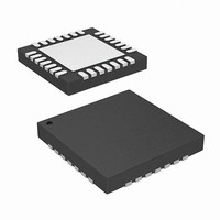
SX1509BULTRT Semtech, SX1509BULTRT Datasheet - Page 10

SX1509BULTRT
Manufacturer Part Number
SX1509BULTRT
Description
IC GPIO EXPANDER I2C 16CH 28QFN
Manufacturer
Semtech
Datasheet
1.SX1508IULTRT.pdf
(41 pages)
Specifications of SX1509BULTRT
Interface
I²C
Number Of I /o
16
Interrupt Output
Yes
Frequency - Clock
400kHz
Voltage - Supply
1.2 V ~ 3.6 V
Operating Temperature
-40°C ~ 85°C
Mounting Type
Surface Mount
Package / Case
28-UTQFN
Includes
LED driver / Keypad Engine
Lead Free Status / RoHS Status
Lead free / RoHS Compliant
Other names
SX1509IULTR
SX1509IULTR
SX1509IULTRT
SX1509IULTR
SX1509IULTRT
Available stocks
Company
Part Number
Manufacturer
Quantity
Price
Company:
Part Number:
SX1509BULTRT
Manufacturer:
Semtech
Quantity:
5 335
ADVANCED COMMUNICATIONS & SENSING
(1) Assuming no load connected to outputs and inputs fixed to VCC1,2 or GND.
(2) Can be increased by tying together and driving simultaneously several I/Os.
(3) All values referred to VIH
(4) A device must internally provide a hold time of at least 300ns for the SDA signal (referred to VIH
the falling edge of SCL.
(5) The maximum t
(6) A Fast-mode I
This will automatically be the case if the device does not stretch the LOW period of the SCL signal.
If such a device does stretch the LOW period of the SCL signal, it must output the next data bit to the SDA line t
= 1250 ns (according to the Standard-mode I2C-bus specification) before the SCL line is released.
(7) C
(8) With RegHighInput bit enabled (VCCx min =1.65V), else 3.6V (VCCx min = 1.2V)
Rev 1 – 30
Symbol
Interface complies with slave F/S mode I
dated January, 2000. Please refer to that document for more detailed I
VOL
IOL
VIH
VIL
f
t
t
t
t
t
t
t
t
t
t
C
V
V
t
Miscellaneous
RPULL
f
SCL
HD;STA
LOW
HIGH
SU;STA
HD;DAT
SU;DAT
r
f
SU;STO
BUF
SP
OSC
nL
nH
b
b
M
M
MR
= total capacitance of one bus line in pF. If mixed with Hs-mode devices, faster fall-times are allowed.
th
Description
Low level output voltage
Low level output sink current
High level input voltage
Low level input voltage
SCL clock frequency
Hold time (repeated) START
condition
LOW period of the SCL clock
HIGH period of the SCL clock
Set-up time for a repeated
START condition
Data hold time
Data set-up time
Rise time of both SDA and SCL
Fall time of both SDA and SCL
Set-up time for STOP condition
Bus free time between a STOP
and START condition
Capacitive load for each bus line
Noise margin at the LOW level
for each connected device
(including hysteresis)
Noise margin at the HIGH level
for each connected device
(including hysteresis)
Pulse width of spikes
suppressed by the input filter
Programmable pull-up/down
resistors for IO[0-7]
Oscillator frequency
Oct. 2009
2
C-bus device can be used in a Standard-mode I
HD;DAT
has only to be met if the device does not stretch the LOW period (t
MR min
and VIL
M max
levels.
Table 6 – Electrical Specifications
2
C interface as described by Philips I
External from OSCIN
VCC1,2 >= 2V
VCC1,2 >= 2V
VDDM >= 2V
2
VCC1,2 < 2V
VCC1,2 < 2V
VDDM < 2V
C-bus system, but the requirement t
Conditions
10
Internal
-
-
-
-
-
-
-
-
-
-
-
-
-
-
-
-
-
World’s Lowest Voltage Level Shifting GPIO
2
C specifications.
with LED Driver and Keypad Engine
20+0.1C
20+0.1C
LOW
VDDM
VDDM
SX1507/SX1508/SX1509
100
) of the SCL signal.
Min
-0.4
0.7*
0.8*
-0.4
-0.4
0.6
1.3
0.6
0.6
0
0.6
1.3
1.3
-
-
-
-
-
-
-
-
-
(4)
(6)
MR min
b
b
2
(7)
(7)
SU;DAT
C specification version 2.1
) to bridge the undefined region of
VDDM
VDDM
Typ
0.1*
0.2*
42
250 ns must then be met.
2
r max
-
-
-
-
-
-
-
-
-
-
-
-
-
-
-
-
-
-
-
-
-
+ t
www.semtech.com
SU;DAT
VDDM
VDDM
0.9
Max
0.3*
0.2*
400
300
300
400
0.3
3.6
3.6
2.6
2.6
= 1000 + 250
50
8
4
-
-
-
-
-
-
-
-
-
-
(5)
mA
kHz
MHz
Unit
k
pF
µs
µs
µs
µs
µs
ns
ns
ns
µs
µs
ns
V
V
V
V
V


