CAT9534HV4I-GT2 ON Semiconductor, CAT9534HV4I-GT2 Datasheet - Page 2
CAT9534HV4I-GT2
Manufacturer Part Number
CAT9534HV4I-GT2
Description
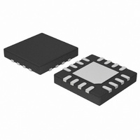
IC I/O EXPANDER 8BIT 16-TQFN
Manufacturer
ON Semiconductor
Datasheet
1.CAT9534YI-GT2.pdf
(16 pages)
Specifications of CAT9534HV4I-GT2
Interface
I²C, SMBus
Number Of I /o
8
Interrupt Output
Yes
Frequency - Clock
400kHz
Voltage - Supply
2.3 V ~ 5.5 V
Operating Temperature
-40°C ~ 85°C
Mounting Type
Surface Mount
Package / Case
16-TFQFN Exposed Pad
Includes
POR
Lead Free Status / RoHS Status
Lead free / RoHS Compliant
Available stocks
Company
Part Number
Manufacturer
Quantity
Price
Company:

Part Number:
CAT9534HV4I-GT2
Manufacturer:
ON Semiconductor
Quantity:
1 400


CAT9534
PIN CONFIGURATION
PIN DESCRIPTION
ABSOLUTE MAXIMUM RATINGS
RELIABILITY CHARACTERISTICS
Notes:
(1) Stresses above those listed under “Absolute Maximum Ratings” may cause permanent damage to the device. These are stress ratings
(2) This parameter is tested initially and after a design or process change that affects the parameter.
(3) Latch-up protection is provided for stresses up to 100mA on address and data pins from -1V to V
Doc. No. MD-9004 Rev. D
Parameters
V
Voltage on Any Pin with Respect to Ground
DC Current on I/O
DC Input Current
V
V
Package Power Dissipation Capability (T
Junction Temperature
Storage Temperature
CC
CC
SS
SOIC / TSSOP
only, and functional operation of the device at these or any other conditions outside of those listed in the operational sections of this
specification is not implied. Exposure to any absolute maximum rating for extended periods may affect device performance and reliability.
Symbol
I
Supply Current
with Respect to Ground
Supply Current
V
LTH
ZAP
(2)(3)
9-12
4-7
13
14
15
16
(2)
1
2
3
8
V
I/O
I/O
I/O
I/O
A0
A1
A2
SS
0
1
2
3
SOIC (W), TSSOP (Y)
Parameter
ESD Susceptibility
Latch-up
0
1
2
3
4
5
6
7
8
to I/O
7
TQFN
7-10
2-5
15
16
11
12
13
14
1
6
16
15
14
13
12
11
10
9
V
SDA
SCL
INT
I/O
I/O
I/O
I/O
CC
7
6
5
4
A
(1)
= 25°C)
Pin Name
Reference Test Method
JEDEC Standard JESD 22
JEDEC Standard 17
I/O
I/O
SDA
SCL
¯¯¯
V
INT
V
A0
A1
A2
2
SS
CC
0-3
4-7
Function
Address Input 0
Address Input 1
Address Input 2
Input/Output Port 0 to Input/Output Port 3
Ground
Input/Output Port 4 to Input/Output Port 7
Interrupt Output (open drain)
Serial Clock
Serial Data
Power Supply
I/O
I/O
I/O
A2
0
1
2
TQFN 4 x 4mm (HV4)
1
2
3
4
A1
I/O
16
5
-0.5 to +6.5
-0.5 to +5.5
-65 to +150
(Top View)
3
CC
Ratings
A0
15
V
6
+150
+1V.
SS
±50
±20
100
1.0
85
Characteristics subject to change without notice
V
I/O
14
7
CC
4
SDA
13
I/O
8
© 2010 SCILLC. All rights reserved
5
2000
12
10
11
Min
100
9
SCL
INT
I/O
I/O
7
6
Units
Units
Volts
mA
mA
mA
mA
mA
ºC
ºC
W
V
V
Related parts for CAT9534HV4I-GT2
Image
Part Number
Description
Manufacturer
Datasheet
Request
R

Part Number:
Description:
ON Semiconductor [VOLTAGE REGULATOR]
Manufacturer:
ON Semiconductor
Datasheet:
Part Number:
Description:
357-036-542-201 CARDEDGE 36POS DL .156 BLK LOPRO
Manufacturer:
ON Semiconductor
Datasheet:
Part Number:
Description:
357-036-542-201 CARDEDGE 36POS DL .156 BLK LOPRO
Manufacturer:
ON Semiconductor
Datasheet:
Part Number:
Description:
357-036-542-201 CARDEDGE 36POS DL .156 BLK LOPRO
Manufacturer:
ON Semiconductor
Datasheet:
Part Number:
Description:
357-036-542-201 CARDEDGE 36POS DL .156 BLK LOPRO
Manufacturer:
ON Semiconductor
Datasheet:
Part Number:
Description:
357-036-542-201 CARDEDGE 36POS DL .156 BLK LOPRO
Manufacturer:
ON Semiconductor
Datasheet:
Part Number:
Description:
357-036-542-201 CARDEDGE 36POS DL .156 BLK LOPRO
Manufacturer:
ON Semiconductor
Datasheet:
Part Number:
Description:
357-036-542-201 CARDEDGE 36POS DL .156 BLK LOPRO
Manufacturer:
ON Semiconductor
Datasheet:
Part Number:
Description:
357-036-542-201 CARDEDGE 36POS DL .156 BLK LOPRO
Manufacturer:
ON Semiconductor
Datasheet:
Part Number:
Description:
357-036-542-201 CARDEDGE 36POS DL .156 BLK LOPRO
Manufacturer:
ON Semiconductor
Datasheet:
Part Number:
Description:
357-036-542-201 CARDEDGE 36POS DL .156 BLK LOPRO
Manufacturer:
ON Semiconductor
Datasheet:
Part Number:
Description:
Manufacturer:
ON Semiconductor
Datasheet:
Part Number:
Description:
Manufacturer:
ON Semiconductor
Datasheet:
Part Number:
Description:
Manufacturer:
ON Semiconductor
Datasheet: