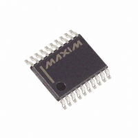
DS4550E+T&R Maxim Integrated Products, DS4550E+T&R Datasheet - Page 9

DS4550E+T&R
Manufacturer Part Number
DS4550E+T&R
Description
IC I/O EXPANDER I2C 9B 20TSSOP
Manufacturer
Maxim Integrated Products
Datasheet
1.DS4550ETR.pdf
(18 pages)
Specifications of DS4550E+T&R
Interface
I²C
Number Of I /o
9
Interrupt Output
No
Frequency - Clock
400kHz
Voltage - Supply
2.7 V ~ 5.5 V
Operating Temperature
-40°C ~ 85°C
Mounting Type
Surface Mount
Package / Case
20-TSSOP
Includes
EEPROM, JTAG
Lead Free Status / RoHS Status
Lead free / RoHS Compliant
The DS4550’s I
state of the A0, A1, and A2 address pins as shown in
Figure
in the corresponding bit position in the slave address.
Conversely, address pins connected to V
‘1’ in the corresponding bit positions. I
tion is described in detail in a later section.
Figure
Figure
TMS
TCK
TDI
3. DS4550 JTAG Block Diagram
2. DS4550 I
R
2. Address pins connected to GND result in a ‘0’
JPU
*THE SLAVE ADDRESS IS DETERMINED BY
MSB
ADDRESS PINS A0, A1, AND A2.
V
1
CC
Slave Address and Address Pins
V
0
CC
2
2
C slave address is determined by the
R
C Slave Address Byte
JPU
1
ADDRESS*
SLAVE
0
A2
MSB
MSB
I
A1
2
C and JTAG Nonvolatile 9-Bit I/O
MEMORY ADDRESS REGISTER
_____________________________________________________________________
BOUNDARY SCAN REGISTER
A0
MEMORY WRITE REGISTER
IDENTIFICATION REGISTER
MEMORY READ REGISTER
INSTRUCTION REGISTER
2
READ/WRITE
TEST ACCESS PORT
[LENGTH = 33 BITS]
[LENGTH = 32 BITS]
(TAP) CONTROLLER
C communica-
[LENGTH = 8 BITS]
[LENGTH = 8 BITS]
BYPASS REGISTER
[LENGTH = 4 BITS]
[LENGTH = 8 BITS]
[LENGTH = 1 BIT]
TEST REGISTERS
CC
R/W
BIT
LSB
result in a
LSB
LSB
Expander Plus Memory
The DS4550 contains an IEEE 1149.1 compliant JTAG
port in addition to the I
to access the internal memory. However, the device
contains no bus arbitration and hence both busses
cannot be used at the same time. All of the I/O pins on
the DS4550 are IEEE 1149.1 boundary-scan compliant.
I/O_0 to I/O_8 as well as the I
typical JTAG boundary scan cells, which allow the pins
to be polled or forced high/low using standard JTAG
instructions. The DS4550 also contains some exten-
sions to normal JTAG functionality, which allows access
to the internal memory. In particular, the DS4550 has
three device-specific test data registers (Memory
Address, Memory Read, and Memory Write) and three
device-specific instructions (ADDRESS, READ, and
WRITE), which provide memory access.
EEPROM
IEEE 1149.1 JTAG Operation
MUX 1
2
C serial bus. Either can be used
MUX 2
2
C port pins, contain the
TDO
9


