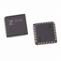
Z0220112VSGR3470 Zilog, Z0220112VSGR3470 Datasheet - Page 13

Z0220112VSGR3470
Manufacturer Part Number
Z0220112VSGR3470
Description
IC MODEM 2400BPS DSP AFE 44-PLCC
Manufacturer
Zilog
Specifications of Z0220112VSGR3470
Data Format
V.21, V.22, V.23, Bell 103, Bell 212A
Baud Rates
2.4k
Interface
Parallel
Voltage - Supply
4.5 V ~ 5.5 V
Mounting Type
Surface Mount
Package / Case
44-LCC (J-Lead)
Lead Free Status / RoHS Status
Lead free / RoHS Compliant
Available stocks
Company
Part Number
Manufacturer
Quantity
Price
Z02201
V.22BIS Data Pump with Integrated AFE
9
supply V
. The HIRQ active Low data pump output can be activated when the
DD
host selects this option or requests by setting the RXIE or TXIE bits in the data
pump Host Register. This pin can be connected to the host interrupt request pin to
initiate host service.
The RESET signal places the device into its
RESET Reset (Input, Active Low)—
reset state.
These three register select lines
HA2–HA0 Host Address (Input, Active High)—
(pins) are used for addressing the controller-accessible internal registers of the
data pump. When HCS is active, the state of the HA2–HA0 is used as the internal
data pump interface register address. HA2 is the most significant bit; HA0 is the
least significant bit.
This pin indicates when
RLSD Receive Line Signal Detect (Output, Active Low)—
an input signal has been detected.
The data pump serial receive data is presented by
RXD Receive Data (Output)—
the data pump to the local DTE on the RXD output.
The serial data output clock is a syn-
TCLK Transmit Serial Data Clock (Output)—
chronous data clock used to transfer serial data via synchronous serial interface
between the data pump and the host. The clock frequencies are 2400, 1200, and
300 Hz, corresponding to the supported data bit rates.
The data pump accepts the serial transmit data from
TXD Transmit Data (Input)—
the local DTE on the TXD input when the data pump is configured to the serial
transmit data mode. The serial transmit data mode is selected when the TDPM bit
(bit 4) of the RAM CONTROL/DATA PUMP STATUS register (Register 6) is reset to
0.
This pin is activated to drive a
OH Off Hook Relay Control (Output, Active Low)—
relay which engages the modem with the phone line (the modem equivalent of
picking up the receiver).
The logical OR of this pin and the
RTS Request To Send (Input, Active Low)—
RTSP bit (bit
of register 4), determines the data pump mode of operation. When
3
the result of the logical OR of these two bits is logic
, the data pump is in transmit
1
mode at the selected speed, thereby placing the data pump in receive mode. In
STANDBY mode, the state of this pin is insignificant.
Data is valid at the rising edge
EYECLK Eye Pattern Clock (Output, Active High)—
of the clock. The EYECLK can be used to clock an external Digital-to-Analog (D/A)
converter shift register for eye pattern display.
This pin controls the serial 16-bit
EYEOUT Eye Pattern Data (Output, Active High)—
eye pattern output data. The first 8 bits is the EYEX data, and the next 8-bits are
the EYEY data. This data can be used for display on an oscilloscope X and Y-axis
following D/A conversion.
PS000904-0107


