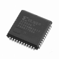
XC9536-7PC44C Xilinx Inc, XC9536-7PC44C Datasheet
XC9536-7PC44C
Specifications of XC9536-7PC44C
Available stocks


Related parts for XC9536-7PC44C


XC9536-7PC44C Summary of contents
Page 1
... Programmable power reduction mode in each macrocell - Slew rate control on individual outputs - User programmable ground pin capability - Extended pattern security features for design protection - High-drive 24 mA outputs - 3. I/O capability Table 1: XC9500 Device Family XC9536 Macrocells 36 Usable Gates 800 Registers 36 T (ns (ns) 3.5 ...
Page 2
... XC9500 In-System Programmable CPLD Family Table 2: Available Packages and Device I/O Pins (not including dedicated JTAG pins) XC9536 44-Pin VQFP 34 44-Pin PLCC 34 48-Pin CSP 34 84-Pin PLCC - 100-Pin TQFP - 100-Pin PQFP - 160-Pin PQFP - 208-Pin HQFP - 352-Pin BGA - 1. Most packages available in Pb-Free option. See individual data sheets for more details. ...
Page 3
... Any number of these product terms the 90 available, can be allocated to each macrocell by the product term allocator. Each FB (except for the XC9536) supports local feedback paths that allow any number of FB outputs to drive into its own programmable AND-array without going outside the FB ...
Page 4
XC9500 In-System Programmable CPLD Family From 36 Fast CONNECT II Switch Matrix 4 Macrocell 1 Product Programmable Term AND-Array Allocators Macrocell 18 1 Global Set/Reset Figure 2: XC9500 Function Block www.xilinx.com 18 To Fast CONNECT II Switch Matrix 18 OUT ...
Page 5
R Macrocell Each XC9500 macrocell may be individually configured for a combinatorial or registered function. The macrocell and associated FB logic is shown in Figure Five direct product terms from the AND-array are available for use as primary data inputs ...
Page 6
XC9500 In-System Programmable CPLD Family All global control signals are available to each individual macrocell, including clock, set/reset, and output enable sig- nals. As shown in Figure 4, the macrocell register clock originates from either of three global clocks or ...
Page 7
R Product Term Allocator The product term allocator controls how the five direct prod- uct terms are assigned to each macrocell. For example, all five direct terms can drive the OR function as shown in Figure 5. Product Term Allocator ...
Page 8
XC9500 In-System Programmable CPLD Family The product term allocator can re-assign product terms from any macrocell within the FB by combining partial sums of products over several macrocells, as shown in In this example, the incremental delay is only 2 ...
Page 9
R The internal logic of the product term allocator is shown in Figure 8. From Upper Macrocell From Lower Macrocell DS063 (v5.5) June 25, 2007 Product Specification XC9500 In-System Programmable CPLD Family To Upper Macrocell Product Term Allocator To Lower ...
Page 10
XC9500 In-System Programmable CPLD Family Fast CONNECT Switch Matrix The Fast CONNECT switch matrix connects signals to the FB inputs, as shown in Figure 9. All IOB outputs (corre- sponding to user pin inputs) and all FB outputs drive the ...
Page 11
R I/O Block The I/O Block (IOB) interfaces between the internal logic and the device user I/O pins. Each IOB includes an input buffer, output driver, output enable selection multiplexer, and user programmable ground control. See details. The input buffer ...
Page 12
XC9500 In-System Programmable CPLD Family Each output has independent slew rate control. Output edge rates may be slowed down to reduce system noise (with an additional time delay of T SLEW ming. See Figure 11. Each IOB provides user programmable ...
Page 13
R In-System Programming XC9500 devices are programmed in-system via a standard 4-pin JTAG protocol, as shown in Figure gramming offers quick and efficient design iterations and eliminates package handling. The Xilinx development sys- tem provides the programming data sequence using ...
Page 14
XC9500 In-System Programmable CPLD Family Figure 13: In-System Programming Operation (a) Solder Device to PCB and (b) Program Using Download Cable Low Power Mode All XC9500 devices offer a low-power mode for individual macrocells or across all macrocells. This feature ...
Page 15
R Combinatorial Logic Propagation Delay = T (a) T PSU Combinatorial Logic P-Term Clock Path Setup Time = T PSU (c) All resources within FB using local Feedback Combinatorial Logic Internal Cycle Time = T ( GCK ...
Page 16
XC9500 In-System Programmable CPLD Family Power-Up Characteristics The XC9500 devices are well behaved under all operating conditions. During power-up each XC9500 device employs internal circuitry which keeps the device in the quiescent state until the V supply voltage is at ...
Page 17
R Table 5: XC9500 Device Characteristics Device Circuitry Device Inputs and Clocks Function Block JTAG Controller Warranty Disclaimer THESE PRODUCTS ARE SUBJECT TO THE TERMS OF THE XILINX LIMITED WARRANTY WHICH CAN BE VIEWED AT http://www.xilinx.com/warranty.htm. THIS LIMITED WARRANTY DOES ...