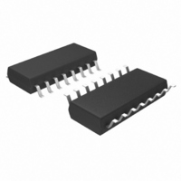
FMA1125DC-16P Fujitsu Semiconductor America Inc, FMA1125DC-16P Datasheet - Page 9

FMA1125DC-16P
Manufacturer Part Number
FMA1125DC-16P
Description
IC CTLR TOUCH SENSOR 16SOP
Manufacturer
Fujitsu Semiconductor America Inc
Type
Capacitiver
Specifications of FMA1125DC-16P
Touch Panel Interface
*
Number Of Inputs/keys
*
Resolution (bits)
*
Data Interface
I²C
Data Rate/sampling Rate (sps, Bps)
*
Voltage Reference
*
Voltage - Supply
2.4 V ~ 5 V
Current - Supply
100µA
Operating Temperature
-40°C ~ 90°C
Mounting Type
Surface Mount
Package / Case
16-SSOP
Output Type
Logic
Interface
I²C
Input Type
Logic
Lead Free Status / RoHS Status
Lead free / RoHS Compliant
Other names
865-1050-2
Table 2. AC Electrical Specifications for I
Notes:
1. All values referred to V
2. A device must internally provide a hold time of al least 300ns for the SDA signal (referred to the V
3. The maximum t
4. A Fast-mode I
5. C
n/a = not applicable.
falling edge of SCL.
case if the device does not stretch the LOW period of the SCL signal. If such a device does stretch the LOW period of the SCL signal, it must output the next data bit
to the SDA line t
b
SDA
SCL
Symbol
t
t
t
t
t
= total capacitance of one bus line in pF. If mixed with Hs-mode devices, faster fall-times according the Table 2 are allowed.
HD:DAT
SU:STO
HD:STA
SU:STA
SU:DAT
t
t
f
f
V
HIGH
V
LOW
SCL
BUF
C
t
t
nL
nH
r
f
b
t
f
2
C-bus device can be used in a Standard-mode I
S
HD:DAT
max
SCL Clock Frequency
Hold Time (repeated) START Condition. After this
Period, the First Clock Pulse is Generated
LOW Period of the SCL Clock
HIGH Period of the SCL Clock
Setup Time for a Repeated START Condition
Data Hold Time:
Data Setup Time
Rise Time of Both SDA and SCL Signals
Fall Time of Both SDA and SCL Signals
Setup Time for STOP Condition
Bus Free Time Between a STOP and START Condition
Capacitive Load for Each Bus Line
Noise Margin at the LOW Level for Each Connected
Device (including Hysteresis)
Noise Margin at the HIGH Level for Each Connected
Device (including Hysteresis)
+ t
For CBUS Compatible Master
For I
has only to be met if the device does not stretch the LOW period (t
IHmin
SU:DAT
t
HD:STA
t
LOW
2
C Bus Devices
and V
= 1,000 + 250 = 1,250ns (according to the Standard-mode I
ILmax
t
r
t
Parameter
SU:DAT
levels (see Table 1).
t
HD:DAT
Figure 6: Definition of Timing for F/S-mode Devices on the I
2
t
C Bus
HIGH
2
C-bus system, but the requirement t
t
f
Confidential
t
SU:STA
0.1 x V
0.2 x V
Min.
250
2
4.0
4.7
4.0
4.7
5.0
4.0
4.7
0
(2)
Standard-Mode
DD
DD
Sr
LOW
2
C bus specification) before the SCL line is released.
) of the SCL signal.
t
HD:STA
3.45
Max.
1000
IHmin
100
300
400
SU:DAT
–
(3)
of the SCL signal) to bridge the undefined regions of the
Š 250ns must then be met. This will automatically be the
2
C-Bus
20 + 0.1C
20 + 0.1C
0.1 x V
0.2 x V
t
100
SP
Min.
0
1.3
0.6
0.6
0.6
1.3
t
0.6
0
–
SU:STO
(2)
(4)
DD
DD
b
b
Fast-Mode
(5)
(5)
FMA1125DC
Fujitsu Microelectronics America, Inc.
t
r
0.9
Max
P
400
300
300
40
–
(3)
t
BUF
S
Unit
kHz
μs
μs
μs
μs
μs
μs
ns
ns
ns
μs
μs
pF
V
V
7


