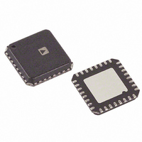
AD9945KCPZ Analog Devices Inc, AD9945KCPZ Datasheet - Page 4

AD9945KCPZ
Manufacturer Part Number
AD9945KCPZ
Description
IC CCD SIGNAL PROCESSOR 32-LFCSP
Manufacturer
Analog Devices Inc
Type
CCD Signal Processor, 12-Bitr
Datasheet
1.AD9945KCPZ.pdf
(14 pages)
Specifications of AD9945KCPZ
Input Type
Logic
Output Type
Logic
Interface
3-Wire Serial
Mounting Type
Surface Mount
Package / Case
32-LFCSP
Ic Function
CCD Signal Processor IC
Supply Voltage Range
2.7V To 3.6V
Operating Temperature Range
-20°C To +85°C
Digital Ic Case Style
LFCSP
No. Of Pins
32
Msl
MSL 3 - 168 Hours
Lead Free Status / RoHS Status
Lead free / RoHS Compliant
Current - Supply
-
Lead Free Status / RoHS Status
Lead free / RoHS Compliant, Lead free / RoHS Compliant
Available stocks
Company
Part Number
Manufacturer
Quantity
Price
Company:
Part Number:
AD9945KCPZ
Manufacturer:
ADI44
Quantity:
300
Part Number:
AD9945KCPZ
Manufacturer:
ADI/亚德诺
Quantity:
20 000
Part Number:
AD9945KCPZRL7
Manufacturer:
ADI/亚德诺
Quantity:
20 000
AD9945
TIMING SPECIFICATIONS
Parameter
SAMPLE CLOCKS
DATA OUTPUTS
SERIAL INTERFACE
*Minimum CLPOB pulse width is for functional operation only. Wider typical pulses are recommended to achieve low noise clamp performance.
Specifications subject to change without notice.
ABSOLUTE MAXIMUM RATINGS*
Parameter
AVDD
DVDD
DRVDD
Digital Outputs
SHP, SHD, DATACLK
CLPOB, PBLK
SCK, SL, SDATA
REFT, REFB, CCDIN
Junction Temperature
Lead Temperature
*Stresses above those listed under Absolute Maximum Ratings may cause perma-
CAUTION
ESD (electrostatic discharge) sensitive device. Electrostatic charges as high as 4000 V readily
accumulate on the human body and test equipment and can discharge without detection. Although the
AD9945 features proprietary ESD protection circuitry, permanent damage may occur on devices
subjected to high energy electrostatic discharges. Therefore, proper ESD precautions are recommended
to avoid performance degradation or loss of functionality.
nent damage to the device. This is a stress rating only; functional operation of the
device at these or any other conditions outside of those indicated in the operational
sections of this specification is not implied. Exposure to absolute maximum ratings
for extended periods may affect device reliability.
(10 sec)
DATACLK, SHP, SHD Clock Period
DATACLK High/Low Pulse Width
SHP Pulse Width
SHD Pulse Width
CLPOB Pulse Width*
SHP Rising Edge to SHD Falling Edge
SHP Rising Edge to SHD Rising Edge
Internal Clock Delay
Output Delay
Pipeline Delay
Maximum SCK Frequency
SL to SCK Setup Time
SCK to SL Hold Time
SDATA Valid to SCK Rising Edge Setup
SCK Falling Edge to SDATA Valid Hold
With
Respect
To
AVSS
DVSS
DRVSS
DRVSS
DVSS
DVSS
DVSS
AVSS
Min Max
–0.3 +3.9
–0.3 +3.9
–0.3 +3.9
–0.3 DVDD + 0.3
–0.3 DVDD + 0.3
–0.3 DVDD + 0.3
–0.3 AVDD + 0.3
–0.3 DRVDD + 0.3 V
(C
L
= 20 pF, f
150
300
SAMP
= 40 MHz, CCD Mode Timing in Figures 8 and 9, Serial Timing in Figures 4 and 5.)
Unit
V
V
V
V
V
V
V
°C
°C
Symbol
t
t
t
t
t
t
t
t
t
f
t
t
t
t
CONV
ADC
SHP
SHD
COB
S1
S2
ID
OD
SCLK
LS
LH
DS
DH
–4–
THERMAL CHARACTERISTICS
Thermal Resistance
32-Lead LFCSP Package
θ
JA
= 27.7 °C/W
Min
25
10
2
11.25
10
10
10
10
10
Typ
12.5
6.25
6.25
20
6.25
12.5
3
9.5
10
Max
Unit
ns
ns
ns
ns
Pixels
ns
ns
ns
ns
Cycles
MHz
ns
ns
ns
ns
REV. B


