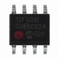
QT110A-ISG Atmel, QT110A-ISG Datasheet

QT110A-ISG
Specifications of QT110A-ISG
Related parts for QT110A-ISG
QT110A-ISG Summary of contents
Page 1
... This device is intended as a replacement for the QT110, consult your local Atmel or Quantum representative See Section 1 on page 2 for differences. and is not recommended for new designs. For further device migration plans please QT110A-ISG R N ECOMMENDED FOR EW Vdd 1 8 Out 2 7 Opt1 3 6 Opt2 ...
Page 2
... OVERVIEW The QT110A is intended to replace the QT110 as a lower cost alternative. This device functions identically to the QT110, except that it is more sensitive. To compensate for the sensitivity increase required to do either of these two things: 1. Increase the Cx loading to ground on SNS2 by 10pF 2. Decrease the Cs value Option 1 is very simple and guarantees that the sensitivity of the QT110A is identical to the older device ...
Page 3
... S ENSITIVITY The QT110A can be set for one of 3 gain levels using option pin 5 (Table 1-1). If left open, the gain setting is high. The sensitivity change is made by altering the numerical threshold level required for a detection also a function of other ...
Page 4
... However, the supply drain is so low simple matter to treat the entire controllable load; simply driving the QT110A's Vdd pin directly from another logic gate or a microprocessor port (Figure 2-2) will serve as both power and 'forced recal'. The source resistance of most CMOS gates and microprocessors is low enough to provide direct power without any problems ...
Page 5
... Out to ground (Figure 2-6). 2.2.6 O The QT110A’s output is active low ; it can source 1mA or sink 5mA of non-inductive current. Care should be taken when the IC and the load are both powered from the same supply, and the supply is minimally regulated ...
Page 6
... Detection ‘stiction’, the opposite effect, can occur if a load is shed when Out is active. The output of the QT110A can directly drive a resistively limited LED. The LED should be connected with its cathode to the output and its anode towards Vcc, so that it lights when the sensor is active-low ...
Page 7
... If there are LEDs or LED wiring near the electrode or its wiring (ie for backlighting of the key), bypass the LED wiring to ground on both its ends. 9. Use a voltage regulator just for the QT110A to eliminate noise coupling from other switching sources via Vdd. Make sure the regulator’s transient load stability provides for a stable voltage just before each burst commences ...
Page 8
... unless otherwise noted. Min Typ Max 3.1 4.7 6. 750 +125 X7R ceramic Notes ms µ 5.0V Vdd ms @ 3.3V Vdd ms ms kHz ms ms µs kHz Units Notes % Note 1 % Note 1 % Note 1 % Note 2 samples ms/level ms/level secs Note 3 QT110A_1R0.01_0408 O C ...
Page 9
... Figure 4-2 Medium Gain Sensitivity and Range @ Vdd = 3V 4.0 3.0 2.0 1.0 Valid Operating Range 10 20 Cs, nF Figure 4-4 Typical Supply Current Vs Vdd Rs = 470K 20pF, Gain = High 20nF 10nF 10 5 2.5 3 3.5 Vdd QT110A_1R0.01_0408 Notes Cx=40pF 35pF 30pF 20pF 15pF 10pF 30 4 4.5 5 ...
Page 10
... W 5.816 Aa 3.81 H 1.371 h 0.101 D 1.27 L 0.355 E 0.508 e 0.19 ß 0.381 Ø 0º ORDERING INFORMATION PART QT110A-ISG LQ Package type: 8-pin SOIC Millimeters Max Notes 4.979 6.198 3.988 1.728 0.762 1.27 BSC 0.483 1.016 0.249 0.762 8º TEMP RANGE PACKAGE -40 - 85C SOIC-8 Lead-Free ...
Page 11
Tel: +44 (0)23 8056 5600 Fax: +44 (0)23 8045 3939 This device covered under one or more of the following United States and international patents: 5,730,165, 6,288,707, 6,377,009, 6,452,514, 6,457,355, 6,466,036, 6,535,200. Numerous further patents are pending which may ...


