AD2S83IP-REEL Analog Devices Inc, AD2S83IP-REEL Datasheet
AD2S83IP-REEL
Specifications of AD2S83IP-REEL


Related parts for AD2S83IP-REEL


AD2S83IP-REEL Summary of contents
Page 1
GENERAL DESCRIPTION The AD2S83 is a monolithic 10-, 12-, 14-, or 16-bit tracking resolver-to-digital converter. The converter allows users to select their own resolution and dynamic performance with external components. The converter allows users to select the resolution to ...
Page 2
... VELOCITY SIGNAL LINEARITY AD2S83AP 0 kHz–500 kHz 0.5 MHz–1 MHz AD2S83IP 0 kHz–500 kHz 0.5 MHz–1 MHz Reversion Error AD2S83AP AD2S83IP 5 DC Zero Offset Gain Scaling Accuracy Output Voltage Dynamic Ripple INPUT/OUTPUT PROTECTION Analog Inputs Analog Outputs DIGITAL POSITION Resolution ...
Page 3
Parameter COMPLEMENT DATA LOAD Sense 6, 7 BUSY Sense Width Load 6 DIRECTION Sense Max Load 6 RIPPLE CLOCK Sense Width Reset Load DIGITAL INPUTS Input High Voltage Input Low Voltage DIGITAL INPUTS Input High Current, ...
Page 4
... Voltage Levels +V S – Current ± ± ± All min and max specifications are guaranteed. Specifications in boldface are tested on all production units at final electrical test. Specifications subject to change without notice. Model AD2S83AP AD2S83IP ( 5 Conditions DB1–DB16 Only ± ± ± ± ...
Page 5
ABSOLUTE MAXIMUM RATINGS (with respect to GND ...
Page 6
AD2S83 Bit Weight Table Binary Resolution Degrees Minutes N Bits ( /Bit /Bit 0 1 360.0 21600 180.0 10800 90.0 5400 45.0 2700 22.5 1350 11.25 675.0 6 ...
Page 7
CONVERTER OPERATION When connected in a circuit such as shown in Figure 10, the AD2S83 operates as a tracking resolver-to-digital converter. The output will automatically follow the input for speeds up to the selected maximum tracking rate. No convert command ...
Page 8
AD2S83 COMPONENT SELECTION The following instructions describe how to select the external components for the converter in order to achieve the required bandwidth and tracking rate. In all cases the nearest “preferred value” component should be used, and a 5% ...
Page 9
Offset Adjust Offsets and bias currents at the integrator input can cause an additional positional offset at the output of the converter of 1 arc minute typical, 5.3 arc minutes maximum. If this can be tolerated, then R8 and ...
Page 10
AD2S83 RIPPLE CLOCK INHIBIT INHIBIT ENABLE SELECT Parameter BUSY ...
Page 11
DIRECTION Output The DIRECTION (DIR) output indicates the direction of the input rotation. Any change in the state of DIR precedes the corresponding BUSY, DATA and RIPPLE CLOCK updates. DIR can be considered as an asynchronous output and can make ...
Page 12
AD2S83 Ratio Multiplier The ratio multiplier is the input section of the AD2S83. This compares the signal from the resolver (angle θ) to the digital (angle φ) held in the counter. Any difference between these two angles results in an ...
Page 13
During the VCO reset period the input continues to be inte- grated. The reset period is constant at 40 ns. The VCO rate is fixed for a given input current by the VCO scaling factor: = 8.5 kHz/µA The tracking ...
Page 14
AD2S83 The small signal step response is shown in Figure 7. The time from the step to the first peak and the t 1 the step until the converter is settled to 1 LSB. The times t ...
Page 15
Ripple Content Ripple content is due to several factors. Tachogenerators suffer from ripple due to the speed of rotation, commutator segments and the number of poles. The resolver/RDC combination has a predominant ripple at twice the resolver reference as a ...
Page 16
AD2S83 SOURCES OF ERRORS Integrator Offset Additional inaccuracies in the conversion of the resolver signals will result from an offset at the input to the integrator. This offset will be treated as an error signal. The resulting angular error will ...
Page 17
Offset Errors The limiting factor in the measuring of low or “creep” speeds is the level of dc offset present at zero velocity. The zero velocity dc offset at the output of the AD2S83 is a function of the input ...
Page 18
AD2S83 APPLICATIONS Control Transformer The ratio multiplier of the AD2S83 can be used independently of the loop integrators as a control transformer. In this mode, the resolver inputs θ are multiplied by a digital angle φ, any difference between φ ...
Page 19
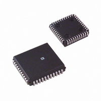
OUTLINE DIMENSIONS Dimensions shown in inches and (mm). Plastic Leaded Chip Carrier (PLCC) (P-44A) 0.180 (4.57) 0.165 (4.19) 0.056 (1.42) 0.048 (1.21) 0.042 (1.07) 0.042 (1.07) 0.048 (1.21 0.042 (1.07 PIN 1 IDENTIFIER TOP VIEW (PINS ...