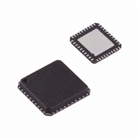
AD9949KCPRL Analog Devices Inc, AD9949KCPRL Datasheet - Page 5

AD9949KCPRL
Manufacturer Part Number
AD9949KCPRL
Description
IC CCD SIGNAL PROCESSOR 40-LFCSP
Manufacturer
Analog Devices Inc
Type
CCD Signal Processor, 12-Bitr
Datasheet
1.AD9949AKCPZ.pdf
(36 pages)
Specifications of AD9949KCPRL
Rohs Status
RoHS non-compliant
Input Type
Logic
Output Type
Logic
Interface
3-Wire Serial
Mounting Type
Surface Mount
Package / Case
40-LFCSP
Analog Front End Type
CCD
Analog Front End Category
Video
Interface Type
Serial (3-Wire)
Sample Rate
36MSPS
Input Voltage Range
0.5V
Operating Supply Voltage (min)
2.7V
Operating Supply Voltage (typ)
3V
Operating Supply Voltage (max)
3.6V
Resolution
12b
Number Of Adc's
1
Power Supply Type
Analog/Digital
Operating Temp Range
-20C to 85C
Operating Temperature Classification
Commercial
Mounting
Surface Mount
Pin Count
40
Package Type
LFCSP EP
Number Of Channels
1
Current - Supply
-
Lead Free Status / RoHS Status
Not Compliant
TIMING SPECIFICATIONS
C
Table 4.
Parameter
MASTER CLOCK (CLI) (See Figure 16)
CLPOB PULSE WIDTH (PROGRAMMABLE)
SAMPLE CLOCKS (See Figure 18)
DATA OUTPUTS (See Figure 19 and Figure 20)
SERIAL INTERFACE (SERIAL TIMING SHOWN IN Figure 14 and Figure 15)
1
Minimum CLPOB pulse width is for functional operation only. Wider typical pulses are recommended to achieve low noise clamp reference.
L
CLI Clock Period
CLI High/Low Pulse Width
Delay from CLI to Internal Pixel Period Position
SHP Rising Edge to SHD Rising Edge
Output Delay From Programmed Edge
Pipeline Delay
Maximum SCK Frequency
SL to SCK Setup Time
SCK to SL Hold Time
SDATA Valid to SCK Rising Edge Setup
SCK Falling Edge to SDATA Valid Hold
SCK Falling Edge to SDATA Valid Read
= 20 pF, f
CLI
= 36 MHz, unless otherwise noted.
1
Rev. B | Page 5 of 36
Symbol
t
t
t
t
t
t
f
t
t
t
t
t
SCLK
CLI
ADC
CLIDLY
COB
S1
OD
LS
LH
DS
DH
DV
Min
27.8
11.2
2
12.5
10
10
10
10
10
10
Typ
13.9
6
20
13.9
6
11
Max
16.6
AD9949
Unit
ns
ns
ns
Pixels
ns
ns
Cycles
MHz
ns
ns
ns
ns
ns


