NCV1124DR2G ON Semiconductor, NCV1124DR2G Datasheet
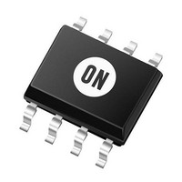
IC SENSOR DUAL VAR-RELUCT 8-SOIC

NCV1124DR2G

Manufacturer Part Number
NCV1124DR2G
Description
IC SENSOR DUAL VAR-RELUCT 8-SOIC
Manufacturer
ON Semiconductor
Type
Variable Reluctancer
Datasheet

Specifications of NCV1124DR2G

Input Type
Logic
Output Type
Logic
Interface
Dual, Serial or Parallel
Current - Supply
5mA
Mounting Type
Surface Mount
Package / Case
8-SOIC (3.9mm Width)
Mounting Style
SMD/SMT
Lead Free Status / RoHS Status
Lead free / RoHS Compliant

Available stocks

Company
Part Number
Manufacturer
Quantity
Price
Part Number:
NCV1124DR2G
Manufacturer:
ON Semiconductor
Quantity:
8 750
Part Number:
NCV1124DR2G
Manufacturer:
ON/安森美
Quantity:
20 000
Part Number:
NCV1124DR2G
0
NCV1124
Dual Variable−Reluctance
Sensor Interface IC
to condition signals from sensors used to monitor rotating parts.
channels interfaces with a variable−reluctance sensor, and
c o n t i n u o u s l y c o m p a r e s t h e s e n s o r o u t p u t s i g n a l t o a
user−programmable internal reference. An alternating input signal of
appropriate amplitude at IN1 or IN2 will result in a rectangular
waveform at the corresponding OUT terminal, suitable for interface to
either standard microprocessors or standard logic families.
test for degradation or loss of the physical connector to both sensors.
Typical Applications
Features
© Semiconductor Components Industries, LLC, 2006
April, 2006 − Rev. 0
The NCV1124 is a monolithic integrated circuit designed primarily
The NCV1124 is a dual channel device. Each of the two identical
A diagnostic input, common to both channels, provides a means to
Anti−Skid Braking and Traction Control
Vehicle Stability Control
Drive Belt Slippage Detection
Crankshaft/Camshaft Position Sensing
Two Independent Channels
Internal Hysteresis
Built−In Diagnostic Mode
Designed to Work from a 5.0 V "10% Supply
Site and Control for Automotive Applications
Pb−Free Packages are Available
R
R
V
V
RS
RS
Variable
Reluctance
Sensor
Variable
Reluctance
Sensor
RS
RS
R1
R2
DIAG
C1
C2
IN1
IN2
V
Figure 1. Block Diagram
CC
INP2
INP1
V
CC
V
CC
Clamp
Clamp
Active
Active
V
CC
IN
Adj
V
R
CC
COMP1
COMP2
Adj
+
+
V
V
GND
CC
CC
1
OUT1
To mP
OUT2
To mP
See detailed ordering and shipping information in the package
dimensions section on page 3 of this data sheet.
V1124
A
L
Y
W
G
ORDERING INFORMATION
GND
IN
MARKING DIAGRAM
IN1
IN2
PIN CONNECTIONS
Adj
http://onsemi.com
1
8
1
= Device Code
= Assembly Location
= Wafer Lot
= Year
= Work Week
= Pb−Free Package
CASE 751
8
SO−8
ALYW4
V1124
Publication Order Number:
G
1
8
V
OUT1
OUT2
DIAG
CC
NCV1124/D

Related parts for NCV1124DR2G

NCV1124DR2G Summary of contents

Page 1

NCV1124 Dual Variable−Reluctance Sensor Interface IC The NCV1124 is a monolithic integrated circuit designed primarily to condition signals from sensors used to monitor rotating parts. The NCV1124 is a dual channel device. Each of the two identical channels interfaces with ...

Page 2

MAXIMUM RATINGS Storage Temperature Range Ambient Operating Temperature Supply Voltage Range (continuous) Input Voltage Range (at any input Maximum Junction Temperature ESD Susceptibility (Human Body Model) Lead Temperature Soldering: Stresses exceeding Maximum Ratings may ...

Page 3

... Output of channel 2 7 OUT1 Output of channel Positive 5.0 volt supply input CC ORDERING INFORMATION Device NCV1124DG NCV1124DR2G †For information on tape and reel specifications, including part orientation and tape sizes, please refer to our Tape and Reel Packaging Specifications Brochure, BRD8011/D. DIAG Variable RS Reluctance ...

Page 4

NORMAL OPERATION Figure 2 shows one channel of the NCV1124 along with the necessary external components. Both channels share the IN pin as the negative input to a comparator. A brief Adj description of the components is as follows: V ...

Page 5

Figure 3 shows the part operating near the minimum input thresholds. As the sin wave input threshold is increased, the low side clamps become active (Figure 4). Increasing the amplitude further (Figure 5), the high−side clamp becomes active. These internal ...

Page 6

Referring to Figure 2, the following will be a design example given these system requirements 1 considered open) V RS(MAX) + 120 RS(MIN) + 250 VRS ...

Page 7

... G C SEATING PLANE −Z− 0.25 (0.010 *For additional information on our Pb−Free strategy and soldering details, please download the ON Semiconductor Soldering and Mounting Techniques Reference Manual, SOLDERRM/D. PACKAGE THERMAL DATA Parameter R qJC R qJA NCV1124 PACKAGE DIMENSIONS SO−8 NB CASE 751−07 ISSUE AG Y ...

Page 8

... Fax: 480−829−7709 or 800−344−3867 Toll Free USA/Canada Email: orderlit@onsemi.com NCV1124 N. American Technical Support: 800−282−9855 Toll Free USA/Canada Japan: ON Semiconductor, Japan Customer Focus Center 2−9−1 Kamimeguro, Meguro−ku, Tokyo, Japan 153−0051 Phone: 81−3−5773−3850 http://onsemi.com 8 ON Semiconductor Website: http://onsemi ...

Related keywords