DS92LV1260TUJB/NOPB National Semiconductor, DS92LV1260TUJB/NOPB Datasheet - Page 2
DS92LV1260TUJB/NOPB
Manufacturer Part Number
DS92LV1260TUJB/NOPB
Description
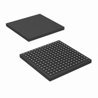
IC DESRL 6CH 10BIT BLVDS 196LBGA
Manufacturer
National Semiconductor
Datasheet
1.DS92LV1260TUJBNOPB.pdf
(17 pages)
Specifications of DS92LV1260TUJB/NOPB
Function
Deserializer
Data Rate
480Mbps
Input Type
LVDS
Output Type
LVTTL
Number Of Inputs
10
Number Of Outputs
1
Voltage - Supply
3 V ~ 3.6 V
Operating Temperature
-40°C ~ 85°C
Mounting Type
Surface Mount
Package / Case
196-LBGA
Lead Free Status / RoHS Status
Lead free / RoHS Compliant
Other names
*DS92LV1260TUJB
*DS92LV1260TUJB/NOPB
DS92LV1260TUJB
*DS92LV1260TUJB/NOPB
DS92LV1260TUJB
Available stocks
Company
Part Number
Manufacturer
Quantity
Price
Company:

Part Number:
DS92LV1260TUJB/NOPB
Manufacturer:
Texas Instruments
Quantity:
10 000


www.national.com
Over recommended operating supply and termperature ranges unless otherwise specified.(Note 2)
LVCMOS/LVTTL DC Specifications:
V
V
V
I
V
V
I
I
Bus LVDS DC specifications
V
V
I
Supply Current
I
I
Timing Requirements for REFCLK
t
t
t
IN
OS
OZ
IN
CCR
CCXR
RFCP
RFDC
RFCP
IH
IL
CL
OH
OL
TH
TL
Symbol
Absolute Maximum Ratings
If Military/Aerospace specified devices are required,
please contact the National Semiconductor Sales Office/
Distributors for availability and specifications.
Electrical Characteristics
Basic functionality and specifications per deserializer channel will be similar to National Semiconductor’s DS92LV1212A.
Supply Voltage (V
Bus LVDS Input Voltage
(Rin +/-)
Maximum Package
Power Dissipation
Package Thermal Resistance
Storage Temp. Range
Junction Termperature
@
25˚C
θ
θ
/t
JA
JC
TCP
196 LBGA:
196 LBGA:
High Level Input Voltage
Low Level Input Voltage
Input Clamp Voltage
Input Current
High Level Output Voltage
Low Level Output Voltage
Output short Circuit Current
TRI-STATE Output Current
Differential Threshold High
Voltage
Differential Threshold Low
Voltage
Input Current
Worst Case Supply Current
Supply Current when
Powered Down
REFCLK Period
REFCLK Duty Cycle
Ratio of REFCLK to TCLK
cc
Parameter
)
V
or REN = 0.8V,
V
V
V
Checker Board
PWRDN= 0.8V
3.6V, 40 MHz,
-65˚C to +150˚C
out
VCM = 1.1V
cc
cc
in
V
V
REN = 0.8V
Conditions
I
PWRDWN
OH
I
(V
out
in
CL=15pF
OL
V
= 0 or 3.6V
Pattern,
-0.3V to 3.9V
= 3.6 or 0V
= 3.6 or 0V
= 0V,(Note
RI+
in
= +2.4V,
V
= -6mA
= 6mA
= 0V or
4)
(Note 1)
CC
=0V,
-0.3 to 4V
-V
34˚C/W
+150˚C
RI-
8˚C/W
3.7W
)
PWRDWN,
SEL (0:2),
Pin/Freq.
REFCLK,
RI+, RI-
RCLK,
LOCK
REN,
R
2
R
OUT
out
Recommended Operating
Conditions
,
Lead Temperature
(Soldering 10 Sec)
ESD Rating:
Reliability Information
Supply Voltage (V
Operating Free Air
Temperature (T
Operating Frequency
Human Body Model
Machine Model
Transistor Count
GND
GND
0.95
Min
-10
-15
-10
-50
-10
-10
2.0
25
40
2
A
)
CC
)
+/-0.2
-0.87
+/- 1
+/- 1
0.18
0.36
Typ
460
-46
+3
50
-2
3
-40˚C to +85˚C
Max
62.5
1.05
V
-1.5
V
+10
+10
+50
+10
+10
530
-85
0.8
0.4
60
CC
CC
1
3.0V to 3.6V
16-40 MHz
+225˚C
>
35,682
>
750V
3KV
Units
mA
mV
mV
mA
mA
uA
uA
uA
uA
ns
%
V
V
V
V
V
Related parts for DS92LV1260TUJB/NOPB
Image
Part Number
Description
Manufacturer
Datasheet
Request
R

Part Number:
Description:
National Semiconductor [8-Bit D/A Converter]
Manufacturer:
National Semiconductor
Datasheet:
Part Number:
Description:
National Semiconductor [Media Coprocessor]
Manufacturer:
National Semiconductor
Datasheet:
Part Number:
Description:
Digitally Controlled Tone and Volume Circuit with Stereo Audio Power Amplifier, Microphone Preamp Stage and National 3D Sound
Manufacturer:
National Semiconductor
Datasheet:
Part Number:
Description:
Digitally Controlled Tone and Volume Circuit with Stereo Audio Power Amplifier, Microphone Preamp Stage and National 3D Sound
Manufacturer:
National Semiconductor
Datasheet:
Part Number:
Description:
AC97 Rev 2 Codec with Sample Rate Conversion and National 3D Sound
Manufacturer:
National Semiconductor
Part Number:
Description:
Manufacturer:
National Semiconductor
Datasheet:
Part Number:
Description:
Manufacturer:
National Semiconductor
Datasheet:
Part Number:
Description:
General Purpose, Low Voltage, Low Power, Rail-to-Rail Output Operational Amplifiers
Manufacturer:
National Semiconductor
Datasheet:
Part Number:
Description:
8-bit 20 MSPS flash A/D converter.
Manufacturer:
National Semiconductor
Datasheet:
Part Number:
Description:
Low Noise Quad Operational Amplifier
Manufacturer:
National Semiconductor
Datasheet:
Part Number:
Description:
Quad Differential Line Receivers
Manufacturer:
National Semiconductor
Datasheet:
Part Number:
Description:
Quad High Speed Trapezoidal? Bus Transceiver
Manufacturer:
National Semiconductor
Datasheet:
Part Number:
Description:
Dual Line Receiver
Manufacturer:
National Semiconductor
Datasheet:
Part Number:
Description:
TTL to 10k ECL Level Translator with Latch
Manufacturer:
National Semiconductor
Datasheet: