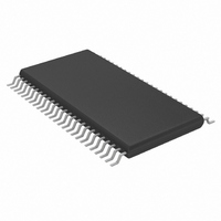
MAX9244EUM+D Maxim Integrated Products, MAX9244EUM+D Datasheet - Page 11

MAX9244EUM+D
Manufacturer Part Number
MAX9244EUM+D
Description
IC DESERIALIZER 21BIT 48-TSSOP
Manufacturer
Maxim Integrated Products
Datasheet
1.MAX9244EUMD.pdf
(23 pages)
Specifications of MAX9244EUM+D
Function
Deserializer
Data Rate
306Mbps
Input Type
LVDS
Output Type
LVTTL, LVCMOS
Number Of Inputs
3
Number Of Outputs
21
Voltage - Supply
3 V ~ 3.6 V
Operating Temperature
-40°C ~ 85°C
Mounting Type
Surface Mount
Package / Case
48-TSSOP
Lead Free Status / RoHS Status
Lead free / RoHS Compliant
28, 36, 48
3, 25, 32,
38, 44
13, 18
19, 21
PIN
10
11
12
14
15
16
17
20
22
23
24
26
27
29
30
31
33
1
2
4
5
6
7
8
9
RxCLKOUT
LVDSGND
RxCLKIN+
RxCLKIN-
PWRDWN
RxOUT17
RxOUT18
RxOUT19
RxOUT20
LVDSV
PLLGND
RxOUT0
RxOUT1
RxOUT2
RxOUT3
RxOUT4
RxOUT5
RxOUT6
PLLV
RxIN0+
RxIN1+
RxIN2+
RxIN0-
RxIN1-
RxIN2-
NAME
V
GND
DCB
SSG
CCO
CC
______________________________________________________________________________________
CC
21-Bit Deserializers with Programmable
Channel 2 Single-Ended Outputs
Ground
Channel 2 Single-Ended Outputs
Three-Level-Logic, Spread-Spectrum Generator Control Input. SSG selects the frequency spread of
RxCLKOUT relative to RxCLKIN_ (see Table 3).
Three-Level-Logic, DC-Balance Control Input. DCB selects DC-balanced, non-DC-balanced, or reserved
operation (see Table 1).
Inverting Channel 0 LVDS Serial-Data Input
Noninverting Channel 0 LVDS Serial-Data Input
Inverting Channel 1 LVDS Serial-Data Input
Noninverting Channel 1 LVDS Serial-Data Input
LVDS Supply Voltage. Bypass LVDSV
the pin as possible.
LVDS Ground
Inverting Channel 2 LVDS Serial-Data Input
Noninverting Channel 2 LVDS Serial-Data Input
Inverting LVDS Parallel-Rate Clock Input
Noninverting LVDS Parallel-Rate Clock Input
PLL Ground
PLL Supply Voltage. Bypass PLLV
the pin as possible.
5V-Tolerant LVTTL/LVCMOS Power-Down Input. PWRDWN is internally pulled down to GND. Outputs are
high impedance when PWRDWN = low or open.
P ar al l el - Rate C l ock S i ng l e- E nd ed O utp ut. The M AX 9242 has a r i si ng - ed g e str ob e. The M AX 9244/M AX 9246/
M AX 9254 have a fal l i ng - ed g e str ob e.
Channel 0 Single-Ended Outputs
Output Supply Voltage. Bypass each V
close to the pin as possible.
Channel 0 Single-Ended Outputs
Spread Spectrum and DC Balance
CC
to GND with 0.1µF and 0.001µF capacitors in parallel as close to
CC
CCO
to GND with 0.1µF and 0.001µF capacitors in parallel as close to
to GND with 0.1µF and 0.001µF capacitors in parallel as
FUNCTION
Pin Description
11


