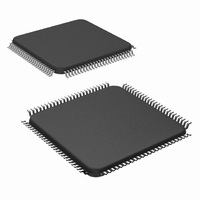
DS90CR483VJDX/NOPB National Semiconductor, DS90CR483VJDX/NOPB Datasheet - Page 19

DS90CR483VJDX/NOPB
Manufacturer Part Number
DS90CR483VJDX/NOPB
Description
IC SERIALIZER 48BIT 100-TQFP
Manufacturer
National Semiconductor
Datasheet
1.DS90CR483VJDNOPB.pdf
(22 pages)
Specifications of DS90CR483VJDX/NOPB
Function
Serializer/Deserializer
Data Rate
5.38Gbps
Input Type
CMOS/TTL
Output Type
LVDS
Number Of Inputs
48
Number Of Outputs
8
Voltage - Supply
3 V ~ 3.6 V
Operating Temperature
-10°C ~ 70°C
Mounting Type
Surface Mount
Package / Case
100-TQFP, 100-VQFP
Lead Free Status / RoHS Status
Lead free / RoHS Compliant
Other names
*DS90CR483VJDX
*DS90CR483VJDX/NOPB
DS90CR483VJDX
*DS90CR483VJDX/NOPB
DS90CR483VJDX
Available stocks
Company
Part Number
Manufacturer
Quantity
Price
Company:
Part Number:
DS90CR483VJDX/NOPB
Manufacturer:
Texas Instruments
Quantity:
10 000
RxINP
RxINM
RxOUT
RxCLKP
RxCLKM
RxCLKOUT
PLLSEL
DESKEW
PD
V
GND
PLLV
PLLGND
LVDSV
LVDSGND
NC
DS90CR484 Pin Description—Channel Link Receiver
Note 13: These receivers have input fail-safe bias circuitry to guarantee a stable receiver output for floating or terminated receiver inputs. Under test conditions
receiver inputs will be in a HIGH state. If the cable interconnect (media) are disconnected which results in floating/terminated inputs, the outputs will remain in the
last valid state.
Note 14: The DS90CR484 is design to automatically detect the DC Balance or non-DC Balance transmitted data from the DS90CR483 and deserialize the LVDS
data according to the define bit mapping.
CC
CC
Pin Name
CC
I/O
O
O
I
I
I
I
I
I
I
I
I
I
I
I
I
Positive LVDS differential data inputs.
Negative LVDS differential data inputs.
TTL level data outputs. In PowerDown (PD = Low) mode, receiver outputs are
forced to a Low state.
Positive LVDS differential clock input.
Negative LVDS differential clock input.
TTL level clock output. The rising edge acts as data strobe.
PLL range select. This pin should be tied to V
NC will force the PLL to low range only. Typical shift point is between 55 and 68
MHz for auto-range. (Notes 11, 12)
Deskew / Oversampling “on/off” select. When using the Deskew / Oversample
feature this pin must be tied to V
(Note 11) Deskew is only supported in the DC Balance mode.
TTL level input. When asserted (low input) the receiver outputs are Low. (Note 11)
Power supply pins for TTL outputs and digital circuitry. Bypass not required on Pins
6 and 77.
Ground pins for TTL outputs and digital circuitry.
Power supply for PLL circuitry.
Ground pin for PLL circuitry.
Power supply pin for LVDS inputs.
Ground pins for LVDS inputs.
No Connect. Make NO Connection to these pins - leave open.
19
CC
. Tieing this pin to ground disables this feature.
Description
CC
for auto-range. Tied to ground or
www.national.com


