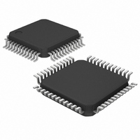
MAX9248ECM/V+T Maxim Integrated Products, MAX9248ECM/V+T Datasheet

MAX9248ECM/V+T
Specifications of MAX9248ECM/V+T
Related parts for MAX9248ECM/V+T
MAX9248ECM/V+T Summary of contents
Page 1
... Navigation System Displays In-Vehicle Entertainment Systems Video Cameras LCD Displays ________________________________________________________________ Maxim Integrated Products For pricing, delivery, and ordering information, please contact Maxim Direct at 1-888-629-4642, or visit Maxim’s website at www.maxim-ic.com. 27-Bit, 2.5MHz to 42MHz DC-Balanced LVDS Deserializers ♦ ...
Page 2
DC-Balanced LVDS Deserializers ABSOLUTE MAXIMUM RATINGS V to _GND........................................................-0.5V to +4.0V CC_ Any Ground to Any Ground...................................-0.5V to +0.5V IN+, IN- to LVDSGND............................................-0.5V to +4.0V IN+, IN- Short Circuit to LVDSGND or V CCLVDS (R/F, OUTEN, ...
Page 3
DC ELECTRICAL CHARACTERISTICS (continued) = +3.0V to +3.6V, PWRDWN = high, differential input voltage ⏐V (V CC_ - ⏐ 2⏐ -40°C to +105°C, unless otherwise noted. Typical values are ...
Page 4
DC-Balanced LVDS Deserializers AC ELECTRICAL CHARACTERISTICS = 8pF, PWRDWN = high, differential input voltage ⏐ +3.0V to +3.6V, C CC_ L = ⏐V - ⏐ 2⏐ 2⏐ ...
Page 5
AC ELECTRICAL CHARACTERISTICS (continued) = 8pF, PWRDWN = high, differential input voltage ⏐ +3.0V to +3.6V, C CC_ L = ⏐V - ⏐ 2⏐ 2⏐ -40°C to +105°C, unless otherwise noted. ...
Page 6
DC-Balanced LVDS Deserializers ( +3.3V 8pF +25°C, unless otherwise noted WORST-CASE PATTERN SUPPLY CURRENT vs. FREQUENCY MAX9248 MAX9250 ...
Page 7
PIN NAME MAX9248 MAX9250 RNG1 CCLVDS LVDSGND 7 7 PLLGND CCPLL 9 9 RNG0 10 10 GND ...
Page 8
DC-Balanced LVDS Deserializers PIN NAME MAX9248 MAX9250 LOCK PCLK_OUT RGB_OUT0– 29–36, 29–36, RBG_OUT7, 39–48 39–48 RGB_OUT8– RGB_OUT17 — 14 OUTEN IN IN- REFCLK PLL SSPLL TIMING AND CONTROL RNG[0:1] 8 ...
Page 9
IN 1. IN- Figure 1. LVDS Input Bias 0 CCO DE_OUT LOCK PCLK_OUT 0 CCO RGB_OUT[17: CNTL_OUT[8:0] Figure 3. Output Rise and Fall Times PCLK_OUT PCLK_OUT SHOWN FOR R/F = ...
Page 10
DC-Balanced LVDS Deserializers PWRDWN REFCLK HIGH IMPEDANCE PCLK_OUT RGB_OUT CNTL_OUT HIGH IMPEDANCE DE_OUT HIGH IMPEDANCE LOCK NOTE: R/F = HIGH Figure 7. PLL Lock to REFCLK and Power-Down Delay for MAX9250 0.8V PWRDWN REFCLK HIGH IMPEDANCE ...
Page 11
OUTEN 0. DE_OUT RGB_OUT[17:0] HIGH IMPEDANCE CNTL_OUT[8:0] Figure 9. Output Enable Time FREQUENCY SSM f (MAX) RxCLKOUT f RxCLKIN f (MIN) RxCLKOUT Figure 11. Simplified Modulation Profile ______________________________________________________________________________________ 27-Bit, 2.5MHz to 42MHz DC-Balanced LVDS Deserializers ...
Page 12
DC-Balanced LVDS Deserializers Detailed Description The MAX9248/MAX9250 DC-balanced deserializers operate at a 2.5MHz-to-42MHz parallel clock frequen- cy, deserializing video data to the RGB_OUT[17:0] out- puts when the data-enable output DE_OUT is high, or control data to ...
Page 13
RGB_IN 1 0 CNTL_IN DE_IN PCLK_IN TIMING AND RNG0 PLL CONTROL RNG1 PWRDWN MAX9247 CERAMIC RF SURFACE-MOUNT CAPACITOR Figure 12. AC-Coupled MAX9247 Serializer and MAX9250 Deserializer with Two Capacitors per Link RGB_IN 1 0 CNTL_IN DE_IN PCLK_IN TIMING AND RNG0 ...
Page 14
DC-Balanced LVDS Deserializers RGB_IN 1 0 CNTL_IN DE_IN PCLK_IN TIMING AND RNG0 PLL CONTROL RNG1 PWRDWN MAX9247 CERAMIC RF SURFACE-MOUNT CAPACITOR *CAPACITORS CAN BE AT EITHER END. Figure 14. AC-Coupled MAX9247 Serializer and MAX9248 Deserializer with ...
Page 15
Input Frequency Detection A frequency-detection circuit detects when the LVDS input is not switching. When not switching, all outputs except LOCK are low, LOCK is high, and PCLK_OUT follows REFCLK. This condition occurs, for example, if the serializer is not ...
Page 16
DC-Balanced LVDS Deserializers Spread-Spectrum Selection The MAX9248 single-ended data and clock outputs are programmable for a variation of ±2% or ±4% around the LVDS input clock frequency. The modulation rate of the frequency variation is 32kHz ...
Page 17
CONTROL DATA PCLK_OUT CNTL_OUT DE_OUT RGB_OUT = OUTPUT DATA HELD Figure 18. Output Timing Staggered and Transition Time Adjusted Outputs RGB_OUT[17:0] are grouped into three groups of six, with each group switching about 1ns apart in the video phase to ...
Page 18
DC-Balanced LVDS Deserializers R D 1MΩ 1.5kΩ CHARGE-CURRENT- DISCHARGE LIMIT RESISTOR RESISTANCE HIGH- C STORAGE VOLTAGE S 100pF CAPACITOR DC SOURCE Figure 19. Human Body ESD Test Circuit R D 2kΩ CHARGE-CURRENT- DISCHARGE LIMIT RESISTOR RESISTANCE ...
Page 19
Chip Information PROCESS: CMOS ______________________________________________________________________________________ 27-Bit, 2.5MHz to 42MHz DC-Balanced LVDS Deserializers For the latest package outline information and land patterns www.maxim-ic.com/packages. PACKAGE TYPE 48 LQFP Package Information PACKAGE CODE DOCUMENT NO. C48+3 21-0054 19 ...
Page 20
... Maxim cannot assume responsibility for use of any circuitry other than circuitry entirely embodied in a Maxim product. No circuit patent licenses are implied. Maxim reserves the right to change the circuitry and specifications without notice at any time. 20 ____________________Maxim Integrated Products, 120 San Gabriel Drive, Sunnyvale, CA 94086 408-737-7600 © 2009 Maxim Integrated Products DESCRIPTION Maxim is a registered trademark of Maxim Integrated Products, Inc ...


