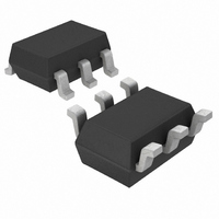
LTC4311CSC6#TRMPBF Linear Technology, LTC4311CSC6#TRMPBF Datasheet - Page 10

LTC4311CSC6#TRMPBF
Manufacturer Part Number
LTC4311CSC6#TRMPBF
Description
IC ACCELERATOR SMBUS DL SC70-6
Manufacturer
Linear Technology
Type
Acceleratorr
Datasheet
1.LTC4311CSC6TRMPBF.pdf
(12 pages)
Specifications of LTC4311CSC6#TRMPBF
Tx/rx Type
I²C Logic
Voltage - Supply
1.6 V ~ 5.5 V
Current - Supply
300µA
Mounting Type
Surface Mount
Package / Case
SC-70-6, SC-88, SOT-363
Lead Free Status / RoHS Status
Lead free / RoHS Compliant
Delay Time
-
Capacitance - Input
-
Other names
LTC4311CSC6#TRMPBF
LTC4311CSC6#TRMPBFTR
LTC4311CSC6#TRMPBFTR
Available stocks
Company
Part Number
Manufacturer
Quantity
Price
APPLICATIONS INFORMATION
LTC4311
The rise time meets the 1μs SMBus requirement and the
fall time meets the 0.3μs requirement. The V
while meeting the minimum slew rate requirements, so R
is chosen to be 13kΩ. If the rise time was not met due to
a large t
value of R
ACK Data Setup Time
Care must be taken in selecting the value of R
with the pull-down driver) to ensure that the data setup
time requirement for ACK (acknowledge) is fulfi lled. An
acknowledge is the host releasing the SDA line (pulling
Table 1. Differences Between LTC1694 and LTC4311
SPECIFICATION
Enable Pin (typ)
V
I
V
I
f
10
CC
PULL-UP
MAX
THRES
CC
In
In
(typ), BUS1, BUS2 High
= 0.156µs
t
t
t
r
2
f
⎧
⎨
⎩
⎧
⎪
⎨
⎪
⎩
= t
= 293Ω • 400pF •
= –13kΩ • 400pF •
(typ)
2.1V + 0.15V – 3.3V – 13kΩ • 2.5mA
(typ)
0.8V – 0.15V
2.1V + 0.15V
1
1
, equation 6 can be used to calculate a maximum
+ t
P
0.9V – 3.3V – 13kΩ • 2.5mA
3.3V
3.3V
that will meet the rise time requirements.
2
= 0.515µs + 0.205µs = 0.72µs
• (13kΩ + 300Ω) – 300Ω
• (13kΩ + 300Ω) – 300Ω
2.7V – 6V
LTC1694
100kHz
2.2mA
0.65V
60μA
N/A
Dependent on V
OL
1.6V – 5.5V
⎫
⎬
⎭
LTC4311
400kHz
S
26μA
= 0.205µs
5mA
is satisfi ed
1V
⎫
⎪
⎬
⎪
⎭
(in series
(20)
(21)
(22)
CC
P
COMMENTS
Allows the LTC4311 to be Disabled, Consuming Less than 5μA
Lower Operating Supply Voltage for Low Voltage Systems
Lower Standby Current to Conserve Power
Tighter, Higher Noise Margins and Improved Rise Times
Stronger Slew-Limited Source Current for Slewing Higher Bus Capacitances
Higher Operating Frequency for I
high) at the end of the last bit sent and the slave device
pulling the SDA line low before the rising edge of the ACK
clock pulse.
The LTC4311 5mA pull-up current is activated when the
host releases the SDA line, allowing the voltage to rise
above the LTC4311’s comparator threshold (V
a slave device has a high value of R
required for the slave device to pull SDA low before the
rising edge of the ACK clock pulse. To ensure suffi cient
data setup time for ACK, slave devices with high values
of R
An alternative is the slave device can hold the SCL line low
until the SDA line reaches a stable state. Then, SCL can
be released to generate the ACK clock pulse.
Multiple LTC4311s in Parallel
In very heavily loaded systems, stronger pull up current
may be desired. Two LTC4311’s may be used in parallel
to increase the total pull up current to meet rise time
requirements.
Notes on Using the LTC4311 in LTC1694 Applications
Although the LTC1694 and LTC4311 are functionally similar
accelerators for I
drain/collector bus applications, the LTC4311 offers a lower
power, higher performance solution in a smaller package
as compared to the LTC1694. These and other differences
are listed in Table 1 and must be accounted for if using
the LTC4311 in LTC1694 applications.
S
should pull the SDA low earlier.
2
C, SMBus, and other comparable open
2
C’s Fast Mode Bus Specifi cation
S
, a longer time is
THR
). If
4311fa


