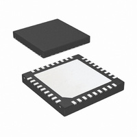
DS25MB100TSQ/NOPB National Semiconductor, DS25MB100TSQ/NOPB Datasheet - Page 3

DS25MB100TSQ/NOPB
Manufacturer Part Number
DS25MB100TSQ/NOPB
Description
IC MUX/BUFFER 1:2 2.5GBPS 36-LLP
Manufacturer
National Semiconductor
Type
MUXr
Datasheet
1.DS25MB100TSQNOPB.pdf
(14 pages)
Specifications of DS25MB100TSQ/NOPB
Tx/rx Type
CML
Delay Time
1.0ns
Voltage - Supply
3.135 V ~ 3.465 V
Mounting Type
Surface Mount
Package / Case
36-LLP
For Use With
DS25MB100EVK - KIT EVAL FOR DS25MB100
Lead Free Status / RoHS Status
Lead free / RoHS Compliant
Current - Supply
-
Capacitance - Input
-
Other names
DS25MB100TSQTR
Available stocks
Company
Part Number
Manufacturer
Quantity
Price
Company:
Part Number:
DS25MB100TSQ/NOPB
Manufacturer:
NSC
Quantity:
895
LINE SIDE HIGH SPEED DIFFERENTIAL IO's
IN+
IN−
OUT+
OUT−
SWITCH SIDE HIGH SPEED DIFFERENTIAL IO's
OUT0+
OUT0−
OUT1+
OUT1−
IN0+
IN0−
IN1+
IN1−
CONTROL (3.3V LVCMOS)
MUX
EQL
EQS
DEL_0
DEL_1
DES_0
DES_1
LB0
LB1
RSV
POWER
V
GND
GND
Pin Name
CC
Pin Descriptions
Note: I = Input, O = Output, P = Power
Note: All CML Inputs or Outputs must be AC coupled.
5, 13, 15, 23,
Pin Number
2, 8, 9, 12,
14, 16, 20,
29, 35
DAP
33
34
30
31
22
21
25
24
19
11
36
18
27
10
28
26
17
32
3
4
6
7
1
I/O
O
O
O
P
P
P
I
I
I
I
I
I
I
I
I
I
Inverting and non-inverting differential inputs at the line side. IN+ and IN− have an internal 50Ω
connected to an internal reference voltage. See Figure 6.
Inverting and non-inverting differential outputs at the line side. OUT+ and OUT− have an internal
50Ω connected to V
Inverting and non-inverting differential outputs at the switch side. OUT0+ and OUT0− have an
internal 50Ω connected to V
Inverting and non-inverting differential outputs at the switch side. OUT1+ and OUT1− have an
internal 50Ω connected to V
Inverting and non-inverting differential inputs to the mux at the switch side. IN0+ and IN0− have
an internal 50Ω connected to an internal reference voltage. See Figure 6.
Inverting and non-inverting differential inputs to the mux at the switch side. IN1+ and IN1− have
an internal 50Ω connected to an internal reference voltage. See Figure 6.
A logic low at MUX selects IN1±. MUX is internally pulled high. Default state for MUX is IN0±.
A logic low enables the input equalizer on the line side. EQL is internally pulled high. Default is
with EQ disabled.
A logic low enables the input equalizer on the switch side. EQS is internally pulled high. Default is
with EQ disabled.
DEL_0 and DEL_1 select the output Pre-emphasis of the line side drivers (OUT±).
DEL_0 and DEL_1 are internally pulled high.
DES_0 and DES_1 select the output Pre-emphasis of the switch side drivers (OUT0±, OUT1±).
DES_0 and DES_1 are internally pulled high.
A logic low at LB0 enables the internal loopback path from IN0± to OUT0±. LB0 is internally pulled
high.
A logic low at LB1 enables the internal loopback path from IN1± to OUT1±. LB1 is internally pulled
high.
Reserve pin to support factory testing. This pin can be left open, or tied to GND, or tied to GND
through an external pull-down resistor.
V
Each V
a via located as close as possible to the landing pad of the V
0.01 μF or 0.1 μF, X7R, size-0402 bypass capacitor from each V
Ground reference. Each ground pin should be connected to the ground plane through a low
inductance path, typically with a via located as close as possible to the landing pad of the GND
pin.
DAP is the metal contact at the bottom side, located at the center of the LLP package. It should
be connected to the GND plane with at least 16 via to lower the ground impedance and improve
the thermal performance of the package.
CC
= 3.3V ± 5%.
CC
pin should be connected to the V
CC
.
CC
CC
3
.
.
Description
CC
plane through a low inductance path, typically with
CC
pin. It is recommended to have a
CC
pin to ground plane.
www.national.com


