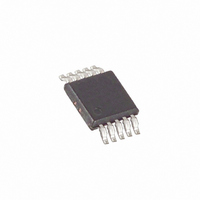
MAX9174EUB+T Maxim Integrated Products, MAX9174EUB+T Datasheet - Page 7

MAX9174EUB+T
Manufacturer Part Number
MAX9174EUB+T
Description
IC SPLITTER 1:2 LVDS 10-UMAX
Manufacturer
Maxim Integrated Products
Type
Splitterr
Datasheet
1.MAX9174EUB.pdf
(14 pages)
Specifications of MAX9174EUB+T
Tx/rx Type
LVDS
Delay Time
2.39ns
Capacitance - Input
4.5pF
Voltage - Supply
3 V ~ 3.6 V
Current - Supply
25mA
Mounting Type
Surface Mount
Package / Case
10-MSOP, Micro10™, 10-uMAX, 10-uSOP
Lead Free Status / RoHS Status
Lead free / RoHS Compliant
The MAX9174/MAX9175 are 670MHz, low-jitter, low-
skew 1:2 splitters ideal for protection switching, loop-
back, and clock and signal distribution. The devices
feature ultra-low 80ps
ensures reliable operation in high-speed links that are
highly sensitive to timing error.
The MAX9174 has a fail-safe LVDS input and LVDS out-
puts. The MAX9175 has an anything differential input
(CML/LVDS/LVPECL) and LVDS outputs. The outputs
can be put into high impedance using the power-down
inputs. The MAX9174 features a fail-safe circuit that dri-
ves the outputs high when the input is open, undriven
and shorted, or undriven and terminated. The MAX9175
has a bias circuit that forces the outputs high when the
input is open. The power-down inputs are compatible
with standard LVTTL/LVCMOS logic.
The power-down inputs tolerate undershoot of -1V and
overshoot of VCC + 1V. The MAX9174/MAX9175 are
available in 10-pin µMAX and 10-lead thin QFN pack-
ages, and operate from a single +3.3V supply over the
-40°C to +85°C temperature range.
The LVDS outputs use a current-steering configuration.
This approach results in less ground bounce and less
output ringing, enhancing noise margin and system
speed performance.
µMAX
10
—
1
2
3
4
5
6
7
8
9
670MHz LVDS-to-LVDS and Anything-to-LVDS
PIN
QFN
EP
10
1
2
3
4
5
6
7
8
9
_______________________________________________________________________________________
Current-Mode LVDS Outputs
P-P
Detailed Description
deterministic jitter (max) that
Exposed
OUT0+
OUT1+
NAME
OUT0-
OUT1-
GND
PD1
PD0
V
Pad
IN+
IN-
CC
Noninverting Differential Input
Inverting Differential Input
Ground
LVTTL/LVCMOS Input. OUT1+, OUT1- are high impedance to ground when PD1 is low.
Internal pulldown resistor to GND.
LVTTL/LVCMOS Input. OUT0+, OUT0- are high impedance to ground when PD0 is low.
Internal pulldown resistor to GND.
Inverting LVDS Output 0
Noninverting LVDS Output 0
Power Supply
Inverting LVDS Output 1
Noninverting LVDS Output 1
Exposed Pad. Solder to ground.
A differential output voltage is produced by steering
current through the parallel combination of the integrat-
ed differential output resistor and transmission line
impedance/termination resistor. When driving a 100Ω
termination resistor, a differential voltage of 250mV to
475mV is produced. For loads greater than 100Ω, the
output voltage is larger, and for loads less than 100Ω,
the output voltage is smaller. See the Differential Output
Voltage vs. Load Resistance curve in Typical Operating
Characteristics for more information. The outputs are
short-circuit current limited for single-ended and differ-
ential shorts.
The fail-safe feature of the MAX9174 sets the outputs
high when the differential input is:
• Open
• Undriven and shorted
• Undriven and terminated
Without a fail-safe circuit, when the input is undriven,
noise at the input may switch the outputs and it may
appear to the system that data is being sent. Open or
undriven terminated input conditions can occur when a
cable is disconnected or cut, or when a driver output is
in high impedance. A shorted input can occur because
of a cable failure.
FUNCTION
MAX9174 Input Fail-Safe
1:2 Splitters
Pin Description
7


