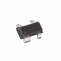
MAX6816EUS+T Maxim Integrated Products, MAX6816EUS+T Datasheet - Page 4

MAX6816EUS+T
Manufacturer Part Number
MAX6816EUS+T
Description
IC DEBOUNCER SWITCH SGL SOT143-4
Manufacturer
Maxim Integrated Products
Datasheet
1.MAX6816EUST.pdf
(8 pages)
Specifications of MAX6816EUS+T
Applications
*
Interface
*
Voltage - Supply
*
Package / Case
SOT-143, SOT-143B, TO-253AA
Mounting Type
Surface Mount
Supply Voltage Range
2.7V To 5.5V
Power Dissipation Pd
320mW
Operating Temperature Range
-40°C To +85°C
Digital Ic Case Style
SOT-143
No. Of Pins
4
Filter Terminals
SMD
Rohs Compliant
Yes
Lead Free Status / RoHS Status
Lead free / RoHS Compliant
±15kV ESD-Protected, Single/Dual/Octal,
CMOS Switch Debouncers
The MAX6816/MAX6817/MAX6818 are designed to
eliminate the extraneous level changes that result from
interfacing with mechanical switches (switch bounce).
Virtually all mechanical switches bounce upon opening
or closing. These switch debouncers remove bounce
when a switch opens or closes by requiring that
sequentially clocked inputs remain in the same state for
a number of sampling periods. The output does not
change until the input is stable for a duration of 40ms.
The circuit block diagram (Figure 1) shows the func-
tional blocks consisting of an on-chip oscillator,
counter, exclusive-NOR gate, and D flip-flop. When the
Figure 1. Block Diagram
4
_______________Detailed Description
MAX6816
_______________________________________________________________________________________
PROTECTION
IN
—
—
—
—
—
—
1
2
3
4
ESD
V
CC
R
PU
MAX6817
PIN
1, 3
4, 6
—
—
—
—
—
—
2
5
V
CC
Theory of Operation
MAX6818
12–19
2–9
10
—
—
—
—
20
11
1
OSC.
OUT2, OUT1
OUT8–OUT1
IN1, IN2
IN1–IN8
NAME
GND
OUT
V
CH
EN
IN
V
CC
CC
D
R
Ground
Switch Input
Switch Inputs
Switch Inputs
CMOS Debounced Output
CMOS Debounced Outputs
CMOS Debounced Outputs
+2.7V to +5.5V Supply Voltage
Active-Low, Three-State Enable Input for outputs. Resets CH.
Tie to GND to “always enable” outputs.
Change-of-State Output. Goes low on switch input change of
state. Resets on EN. Leave unconnected if not used.
COUNTER
input does not equal the output, the XNOR gate issues
a counter reset. When the switch input state is stable
for the full qualification period, the counter clocks the
flip-flop, updating the output. Figure 2 shows the typical
opening and closing switch debounce operation. On
the MAX6818, the change output (CH) is updated
simultaneously with the switch outputs.
The undervoltage lockout circuitry ensures that the out-
puts are at the correct state on power-up. While the sup-
ply voltage is below the undervoltage threshold
(typically 1.9V), the debounce circuitry remains trans-
parent. Switch states are present at the logic outputs
with no debouce delay.
Q
LOCKOUT
VOLTAGE
UNDER-
D
LOAD
FUNCTION
Q
Undervoltage Lockout
Pin Description
MAX6816
MAX6817
MAX6818
OUT


