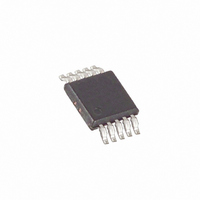
MAX1840EUB+ Maxim Integrated Products, MAX1840EUB+ Datasheet - Page 2

MAX1840EUB+
Manufacturer Part Number
MAX1840EUB+
Description
IC TRANS LEVEL SIM 10-UMAX
Manufacturer
Maxim Integrated Products
Datasheet
1.MAX1840EUB.pdf
(8 pages)
Specifications of MAX1840EUB+
Applications
Smart Card
Interface
MICROWIRE™, QSPI™, Serial, SPI™
Voltage - Supply
1.4 V ~ 5.5 V, 1.7 V ~ 5.5 V
Package / Case
10-TFSOP, 10-MSOP (0.118", 3.00mm Width)
Mounting Type
Surface Mount
Maximum Operating Temperature
+ 85 C
Minimum Operating Temperature
- 40 C
Mounting Style
SMD/SMT
Lead Free Status / RoHS Status
Lead free / RoHS Compliant
ABSOLUTE MAXIMUM RATINGS
DV
RIN, CIN, DATA, DDRV,
RST, CLK, IO to GND .................................-0.3V to (V
Continuous Power Dissipation (T
Low-Voltage SIM/Smart Card
Level Translators in µMAX
Stresses beyond those listed under “Absolute Maximum Ratings” may cause permanent damage to the device. These are stress ratings only, and functional
operation of the device at these or any other conditions beyond those indicated in the operational sections of the specifications is not implied. Exposure to
absolute maximum rating conditions for extended periods may affect device reliability.
ELECTRICAL CHARACTERISTICS
(Figure 1, DV
C
2
POWER SUPPLIES
CIN, RIN, SHDN, DDRV LOGIC INPUTS
CLK, RST OUTPUTS
DATA INPUT/OUTPUT
DV
V
DV
V
Total Shutdown Current
Digital Input Low Threshold
Digital Input High Threshold
Input Leakage Current
Digital Output Low Level
Digital Output High Level
DATA Pullup Resistance
Input Low Threshold
Input High Threshold
Input Low Current
Input High Current
IO
SHDN to GND ......................................-0.3V to (DV
10-Pin µMAX (derate 5.6mW/°C above +70°C) ...........444mW
CC
CC
CC
= C
_______________________________________________________________________________________
CC
CC
, V
Operating Range
Operating Current
Operating Range
Operating Current
CLK
CC
PARAMETER
to GND................................................-0.3V to +6.0V
= C
CC
RST
= +1.8V; V
= C
DATA
CC
= 30pF, T
= +1.8V, +3.0V, or +5.0V; SHDN = DV
A
= +70°C)
SYMBOL
V
V
IH(DATA)
R
IL(DATA)
I
I
DV
DVCC
I
SHDN
V
V
V
A
VCC
V
DATA
V
I
I
CC
OH
IH
OL
IL
IH
IL
CC
= -40°C to +85°C, unless otherwise noted. Typical values are at T
CIN static
CIN clocked at 1.625MHz from GND to DV
with 50% duty cycle
CIN clocked at 3.25MHz from GND to DV
with 50% duty cycle
CIN static
CIN clocked at 1.625MHz from GND to DV
with 50% duty cycle
CIN clocked at 3.25MHz from GND to DV
with 50% duty cycle
I
(MAX1840 only), or DV
or V
I
I
I
Between DATA and DV
(Note 2)
(Note 3)
V
OFF
SINK
SOURCE
SOURCE
CC
CC
= 5.0V
= I
CC
CC
= 200µA
= GND
VCC
+ 0.3V)
+ 0.3V)
= 20µA
= 200µA
+ I
DVCC
CONDITIONS
, SHDN = GND
CC
Operating Temperature Range ...........................-40°C to +85°C
Storage Temperature Range .............................-65°C to +150°C
Junction Temperature ......................................................+150°C
Lead Temperature (soldering, 10s) .................................+300°C
CC
, CIN = RIN = GND or DV
CC
= GND
CC
CC
CC
CC
0.2
0.9
0.8
CC
MIN
1.4
1.7
0.3
13
, IO = V
✕
✕
✕
DV
V
V
CC
CC
CC
A
CC
= +25°C.) (Note1)
TYP
0.01
0.01
0.1
2.5
0.9
0.4
0.8
20
5
, DATA = DDRV = DV
0.7
DV
CC
✕
MAX
0.5
3.0
0.4
28
5.5
5.5
1
DV
1
1
2
- 0.6
CC
UNITS
mA
mA
µA
µA
µA
µA
kΩ
µA
V
V
V
V
V
V
V
V
CC
,


