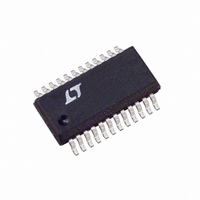
LTC1755EGN Linear Technology, LTC1755EGN Datasheet - Page 7

LTC1755EGN
Manufacturer Part Number
LTC1755EGN
Description
IC SMART CARD INTERFACE 24SSOP
Manufacturer
Linear Technology
Datasheet
1.LTC1756EGNPBF.pdf
(16 pages)
Specifications of LTC1755EGN
Applications
Smart Card
Voltage - Supply
2.7 V ~ 6 V
Package / Case
24-SSOP
Mounting Type
Surface Mount
Lead Free Status / RoHS Status
Contains lead / RoHS non-compliant
Interface
-
Available stocks
Company
Part Number
Manufacturer
Quantity
Price
Company:
Part Number:
LTC1755EGN
Manufacturer:
MOT
Quantity:
2 137
Part Number:
LTC1755EGN
Manufacturer:
LT/凌特
Quantity:
20 000
Part Number:
LTC1755EGN#PBF
Manufacturer:
LT凌特厂
Quantity:
20 000
PI FU CTIO S
Note: If a normally closed switch is used, a small current
(several microamperes) will flow through the switch when-
ever a Smart Card is not present. For ultralow power
consumption in shutdown, a normally open switch is
optimum.
DV
GND (Pins 5/3): Ground Reference for the IC. This pin
should be connected to a low impedance ground plane.
Bypass capacitors for V
proximity to the GND pin.
V
be between 2.7V and 6V. A 10 F low ESR ceramic bypass
capacitor is required on this pin for optimum performance.
V
This pin should be connected to the Smart Card V
contact. The 5V/3V pin determines the V
The V
ing the actual output voltage with an internal reference
voltage. If V
the LTC1755/LTC1756 switch to the Alarm state (see the
State Diagram). The V
storage capacitor to ground. For optimum performance a
low ESR ceramic capacitor should be used.
During the Idle and Alarm states the V
discharged to ground to comply with the deactivation
requirements of the EMV and ISO-7816 specifications.
AUX1 (Pin 8, LTC1755 Only): (Input/Output) Smart Card
Side Auxiliary I/O Pin. This pin is used for auxiliary
bidirectional data transfer between the microcontroller
and the Smart Card. It has the same characteristics as the
I/O pin.
AUX2 (Pin 9, LTC1755 Only): (Input/Output) Smart Card
Side Auxiliary I/O Pin. This pin is used for auxiliary
bidirectional data transfer between the microcontroller
and the Smart Card. It has the same characteristics as the
I/O pin.
I/O (Pins 10/6): (Input/Output) Smart Card Side Data I/O
Pin. This pin is used for bidirectional data transfer between
the microcontroller and the Smart Card. It should be con-
nected to the Smart Card I/O contact. The Smart Card I/O
pin must be able to sink up to 250 A when driving the I/O
IN
CC
CC
U
(Pins 6/4): Supply Voltage for the Charge Pump. May
(Pins 7/5): Regulated Smart Card Supply Voltage.
CC
sets the logic reference level for the NC/NO pin.
pin is protected against short circuits by compar-
U
CC
is below its correct level (for as little as 5 s)
U
CC
IN
LTC1755/LTC1756
pin requires a 10 F charge
and V
CC
should be in close
CC
CC
output voltage.
pin is rapidly
CC
pin low due to the pull-up current source. The I/O pin be-
comes a low impedance to ground during the Idle state. It
does not become active until READY goes low indicating
that V
Once READY is low the I/O pin is protected against short
circuits to V
The DATA-I/O channel is bidirectional for half-duplex
transmissions. Its idle state is H-H. Once an L is detected
on one side of the channel the direction of transmission is
established. Specifically, the side which received an L first
is now the input, and the opposite side is the output.
Transmission from the output side back to the input side
is inhibited, thereby preventing a latch condition. Once the
input side releases its L, both sides return to H, and the
channel is now ready for a new L to be transmitted in either
direction. If an L is forced externally on the output side, and
it persists until after the L on the input side is released, this
illegal input will not be transmitted to the input side
because the transmission direction will not have changed.
The direction of transmission can only be established from
the idle (H-H) state and is determined by the first receipt
of an L on either side.
RST (Pins 11/7): (Output) Level-Shifted Reset Output Pin.
This pin should be connected to the Smart Card RST
contact. The RST pin becomes a low impedance to ground
during the Idle state (see the State Diagram). The reset
channel does not become active until the READY signal
goes low indicating that V
Short-circuit protection is provided on the RST pin by
comparing RST with R
microseconds then the LTC1755/LTC1756 switch to the
Alarm state. This fault checking is only performed after the
V
READY pin).
CLK (Pins 12/8): (Output) Level-Shifted Clock Output Pin.
This pin should be connected to the Smart Card CLK
contact. The CLK pin becomes a low impedance to ground
during the Idle state (see the State Diagram). The clock
channel does not become active until the READY signal
goes low indicating that V
Short-circuit protection is provided on the CLK pin by
comparing CLK with C
CC
pin has reached its final value (as indicated by the
CC
is stable.
CC
by current limiting to 5mA maximum.
IN
IN
LTC1755/LTC1756
. If these signals differ for several
. If these signals differ for several
CC
CC
is stable.
is stable.
7


