MCZ33990EFR2 Freescale Semiconductor, MCZ33990EFR2 Datasheet
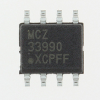
MCZ33990EFR2
Specifications of MCZ33990EFR2
Available stocks


Related parts for MCZ33990EFR2

MCZ33990EFR2 Summary of contents
Page 1
... Capability BAT • Pb-Free Packaging Designated by Suffix Code EF V BAT MCU Freescale Semiconductor, Inc. reserves the right to change the detail specifications, as may be required, to permit improvements in the design of its products. © Freescale Semiconductor, Inc., 2006-2008. All rights reserved. MC33990D/DR2 MCZ33990EF/R2 33990 +VBAT ...
Page 2
... Note This device contains approximately 400 active transistors and 250 gates. Figure 2. 33990 Simplified Internal Block Diagram 33990 2 INTERNAL BLOCK DIAGRAM 33990 Voltage Regulator Waveshaping Filter 4X Enable Loopback Bus BUS Driver Thermal Shutdown Loss of Ground LOAD Protection GND Analog Integrated Circuit Device Data Freescale Semiconductor ...
Page 3
... Tristate input mode control; Logic 0 = normal waveshaping, Logic 1 = waveshaping disabled for 4X 6 4X/ LOOP transmitting, high impedance = loopback mode. Serial data input (DI) from the microcontroller to be transmitted onto Bus Bus received serial data output (DO) sent to the microcontroller Analog Integrated Circuit Device Data Freescale Semiconductor PIN CONNECTIONS SLEEP GND ...
Page 4
... PPRT R θ J-A = 100 pF, R ZAP = 200 pF, R ZAP Value Unit - -0.3 to 7 ±2000 ±200 °C -65 to 150 °C -40 to 125 °C -40 to 150 °C Note 6. 180 ° 1500 Ω). ZAP = 0 Ω). ZAP Analog Integrated Circuit Device Data Freescale Semiconductor ...
Page 5
... Typical threshold value is the approximate actual occurring switch point value with V 8. Device characterized but not production tested for thermal shutdown. 9. Device characterized but not production tested for thermal shutdown hysteresis. Analog Integrated Circuit Device Data Freescale Semiconductor ≤ -40°C ≤ T ≤ 125°C, BAT A Symbol ...
Page 6
... All positive currents A Typ Max Unit mA – 0.5 V 0.07 0.2 V 0.67 0.9 V 2.27 0.8 2.27 – µA 120 200 -0.1 2.0 µA -95 – 95 200 V 1.6 1.8 3.43 3.6 V 0.18 0.4 V 4.48 4.75 mA 5.9 8.0 V 4.56 4.85 µA -0.003 -2.0 9.5 20 Freescale Semiconductor ...
Page 7
... Figure 10) Low-to-Output High High-to-Output Low Notes 10. Typical is the parameter's approximate average value with V 11. RX Output Transition Time from a sleep state. Analog Integrated Circuit Device Data Freescale Semiconductor ≤ -40°C ≤ T ≤ 125°C, BAT A Symbol ≤ 7.812 kHz Square t rise (BUS) t fall (BUS) ≤ ...
Page 8
... BUS Rx 64 μs t pwd(min) t pwd t pwd(max) Figure 7. Pulse Width Distortion 2 SLEEPTxSU 2 3.875 V TxDelay Figure Delay Times SLEEP 122 μs 3.875 V t RxDelay / low- to-output high t RxDelay /high-to- output low 2.5 V Figure 9. BUS-to-Rx Delay Time Analog Integrated Circuit Device Data Freescale Semiconductor ...
Page 9
... RxTrans L–H / 90% Rx 10% Figure 10. Rx Rise and Fall Time Analog Integrated Circuit Device Data Freescale Semiconductor t RxTrans H–L / 90% 10% ELECTRICAL CHARACTERISTICS TEST FIGURES 33990 9 ...
Page 10
... Figure 12. Maximum Number of Nodes ≤ 125°C and 7.0 V ≤ BAT Figure 13). All nodes Table 6. One Primary Node 470 pF 1.5 kΩ 3300 pF Primary Node 3300 pF 470 pF 1.5 kΩ 24 Secondary Nodes 442 Ω 11280 pF Analog Integrated Circuit Device Data Freescale Semiconductor ≤ ...
Page 11
... Table 6. Class B Bus Capacitance and Resistance Expressions Level Minimum (3.3 x 0.9) + (0.47 x 0.9) = 3.39 nF Maximum (3 (0.47 x 1.1) = 16.55 nF Analog Integrated Circuit Device Data Freescale Semiconductor 14570 pF Capacitance (1.5 x 0.95) || (10.6 x 0.95 314 Ω (1.5 x 1.05) || (10.6 x 1.05) = 1.38 kΩ FUNCTIONAL DESCRIPTION FUNCTIONAL PIN DESCRIPTION ...
Page 12
... The microcontroller provides the VPW decoding function. Once the receiver detects a transition on Rx, it starts an internal counter. The initial “start of frame” bit is a logic [1] and lasts 200 μs. For subsequent bits, if there is a bus . This BAT DD Analog Integrated Circuit Device Data Freescale Semiconductor ...
Page 13
... V BAT MCU Analog Integrated Circuit Device Data Freescale Semiconductor and biased “off” when loss-of-ground occurs. When a loss of assembly ground occurs, the load transistor switch is self- biased “off”, allowing no more than 100 μA of leakage current to flow in the LOAD pin. During such a loss of assembly ...
Page 14
... PACKAGING PACKAGE DIMENSIONS For the most current package revision, visit www.freescale.com and perform a keyword search using the “98A” listed below. 33990 14 PACKAGING PACKAGE DIMENSIONS D SUFFIX EF SUFFIX (PB-FREE) 8-PIN PLASTIC PACKAGE 98ASB42564B Analog Integrated Circuit Device Data Freescale Semiconductor ...
Page 15
... Changed status to final, “Technical Data” thereby removing the “Advance Information” watermark 10/2008 4.0 on page 1. No Technical Changes. Analog Integrated Circuit Device Data Freescale Semiconductor REVISION HISTORY 4. Added note with instructions to obtain this information from REVISION HISTORY 33990 15 ...
Page 16
... Freescale Semiconductor product could create a situation where personal injury or death may occur. Should Buyer ...