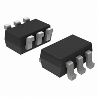
NLASB3157DFT2G ON Semiconductor, NLASB3157DFT2G Datasheet - Page 4

NLASB3157DFT2G
Manufacturer Part Number
NLASB3157DFT2G
Description
IC SWITCH SPDT SC88
Manufacturer
ON Semiconductor
Type
Analog Switchr
Datasheet
1.NLASB3157DFT2G.pdf
(10 pages)
Specifications of NLASB3157DFT2G
Function
Switch
Circuit
1 x SPDT
On-state Resistance
7 Ohm
Voltage Supply Source
Single Supply
Voltage - Supply, Single/dual (±)
1.65 V ~ 5.5 V
Current - Supply
1µA
Operating Temperature
-55°C ~ 125°C
Mounting Type
Surface Mount
Package / Case
6-TSSOP, SC-88, SOT-363
Multiplexer Configuration
Single SPDT
Number Of Inputs
1
Number Of Outputs
2
Number Of Channels
1
Analog Switch On Resistance
50@1.65VOhm
Analog Switch Turn On Time
23ns
Analog Switch Turn Off Time
12.5ns
Package Type
SOT-363
Power Supply Requirement
Single
Single Supply Voltage (min)
1.65V
Single Supply Voltage (typ)
3/5V
Single Supply Voltage (max)
5.5V
Dual Supply Voltage (min)
Not RequiredV
Dual Supply Voltage (typ)
Not RequiredV
Dual Supply Voltage (max)
Not RequiredV
Power Dissipation
180mW
Mounting
Surface Mount
Pin Count
6
Operating Temp Range
-55C to 125C
Operating Temperature Classification
Military
Lead Free Status / RoHS Status
Lead free / RoHS Compliant
Other names
NLASB3157DFT2GOSTR
Available stocks
Company
Part Number
Manufacturer
Quantity
Price
Company:
Part Number:
NLASB3157DFT2G
Manufacturer:
ON
Quantity:
6 000
Part Number:
NLASB3157DFT2G
Manufacturer:
ON/安森美
Quantity:
20 000
8. Guaranteed by Design.
9. This parameter is guaranteed by design but not tested. The bus switch contributes no propagation delay other than the RC delay of the On
10. Off Isolation = 20 log
11. T
AC ELECTRICAL CHARACTERISTICS − NLASB3157
CAPACITANCE − NLASB3157
Symbol
t
t
t
t
t
t
t
Q
OIRR
Xtalk
BW
THD
C
C
C
PHL
PLH
PZL
PZH
PLZ
PHZ
B−M
Symbol
IN
IO−B
IOA−ON
Resistance of the switch and the 50 pF load capacitance, when driven by an ideal voltage source (zero output impedance).
A
= +25°C, f = 1 MHz, Capacitance is characterized but not tested in production.
Propagation Delay
Bus to Bus (Note 9)
Output Enable Time
Turn On Time
(A to B
Output Disable Time
Turn Off Time
(A Port to B Port)
Break Before Make
Time (Note 8)
Charge Injection
(Note 8)
Off Isolation (Note 10)
Crosstalk
−3 dB Bandwidth
Total Harmonic
Distortion (Note 8)
Select Pin Input Capacitance
B Port Off Capacitance
A Port Capacitance when Switch is Enabled
Parameter
n
)
10
[V
A
/V
Bn
Parameter
].
V
V
V
V
V
C
R
R
f = 10 MHz
R
f = 10 MHz
R
R
0.5 V
f = 600 Hz to 20 kHz
(Note 11)
I
I
I
I
I
L
GEN
L
L
L
L
= 2
= 2
= OPEN
= 0 V for t
= 0 V for t
= 0.1 nF, V
= 50 W
= 50 W
= 50 W
= 600 W
Test Conditions
P−P
= 0 W
V
V
CC
CC
PZH
PHZ
GEN
for t
for t
PZL
PLZ
= 0 V
http://onsemi.com
V
V
V
1.65−1.95
1.65−1.95
1.65−1.95
1.65−1.95
1.65−5.5
1.65−5.5
1.65−5.5
2.3−2.7
3.0−3.6
4.5−5.5
2.3−2.7
3.0−3.6
4.5−5.5
2.3−2.7
3.0−3.6
4.5−5.5
2.3−2.7
3.0−3.6
4.5−5.5
CC
CC
CC
V
(V)
5.0
3.3
5.0
CC
= 0 V
= 5.0 V
= 5.0 V
4
Test Conditions
Min
T
A
= +255C
0.011
Typ
−57
−54
250
7.0
3.0
Max
12.5
6.9
5.2
7.0
5.0
3.5
23
13
18.5
T
Typ
2.3
6.5
A
Min
7.0
3.5
2.5
1.7
3.0
2.0
1.5
0.8
0.5
0.5
0.5
0.5
= −405C to +855C
Max
Max
1.2
0.8
0.3
7.6
5.7
7.5
5.3
3.8
24
14
13
Unit
pF
pF
pF
Unit
MHz
pC
dB
dB
ns
ns
ns
ns
%
Number
Figure 8
Figure 9
Figure 10
Figure
Number
Figure 4
Figure 5
Figure 6
Figure 7
Figures
Figures
Figures
Figure
2, 3
2, 3
2, 3


