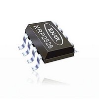
XRP2526ID-1-F Exar Corporation, XRP2526ID-1-F Datasheet - Page 2

XRP2526ID-1-F
Manufacturer Part Number
XRP2526ID-1-F
Description
Power Switch ICs - USB DUAL CH USB SWITCH ACTIVE HIGH
Manufacturer
Exar Corporation
Series
-r
Type
High Side Switchr
Datasheet
1.XRP2525ID-2-F.pdf
(11 pages)
Specifications of XRP2526ID-1-F
Supply Voltage (max)
5.5 V
Supply Voltage (min)
1.8 V
Maximum Operating Temperature
+ 85 C
Minimum Operating Temperature
- 40 C
Package / Case
SOIC-8
Number Of Switches
Dual
Off Time (max)
22 us
On Time (max)
2000 us
Supply Current
80 uA
Number Of Outputs
2
Rds (on)
140 mOhm
Internal Switch(s)
Yes
Current Limit
900mA
Voltage - Input
1.75 V ~ 5.5 V
Operating Temperature
-40°C ~ 85°C
Mounting Type
Surface Mount
Lead Free Status / Rohs Status
Details
Available stocks
Company
Part Number
Manufacturer
Quantity
Price
Company:
Part Number:
XRP2526ID-1-F
Manufacturer:
EXAR
Quantity:
5 000
Part Number:
XRP2526ID-1-F
Manufacturer:
EXAR/艾科嘉
Quantity:
20 000
ABSOLUTE MAXIMUM RATINGS
These are stress ratings only and functional operation of
the device at these ratings or any other above those
indicated in the operation sections of the specifications
below is not implied. Exposure to absolute maximum
rating conditions for extended periods of time may affect
reliability.
V
V
Storage Temperature .............................. -65°C to 150°C
Power Dissipation ................................ Internally Limited
Lead Temperature (Soldering, 10 sec) ................... 300°C
ESD Rating (HBM - Human Body Model) .................... 2kV
ESD Rating (MM - Machine Model) ........................... 200V
ELECTRICAL SPECIFICATIONS
Specifications are for an Operating Junction Temperature of T
Temperature range are denoted by a “•”. Minimum and Maximum limits are guaranteed through test, design, or statistical
correlation. Typical values represent the most likely parametric norm at T
only. Unless otherwise indicated, 1.8V to 5.5V, C
© 2011 Exar Corporation
Input Supply Voltage
Input Quiescent Current
Input Quiescent Current
Input Shutdown Current
Maximum Output Current per
channel
Output Leakage Current
Reverse Leakage Current
Output MOSFET Resistance
Output turn-on delay
Output turn-on rise time
Output turn-off delay
Output turn-off fall time
Current limit threshold
Short Circuit Current Limit
Output Voltage Short Circuit
Detect Threshold
Safe Operating Area (SOA)
Current Limit
Over temperature shutdown
threshold
Over temperature shutdown
threshold hysteresis
Under-voltage lockout threshold
Under-voltage lockout hysteresis
FLG output logic low voltage
FLG output high leakage
FLG blanking time
EN input logic high voltage
EN input logic low voltage
EN input leakage current
IN
EN
........................................................... -0.3V to 7.0V
, V
FLG
............................................................... 7.0V
Parameter
S
S
i
i
n
n
g
Min.
g
0.90
1.55
900
1.8
1.5
-1
l
l
e
e
/
/
D
D
0.66xI
u
u
1000
2000
Typ.
1.15
1.68
925
135
100
a
a
80
52
80
10
22
10
50
10
IN
3
0
l
l
= 47µF//1µF, C
LIM
C
C
h
h
a
a
Max.
4000
1.40
1.75
n
150
100
140
250
n
5.5
0.5
10
10
20
50
2/11
3
1
1
n
n
J
e
e
= 25°C only; limits applying over the full Operating Junction
l
l
OPERATING RATINGS
Input Voltage Range V
Junction Temperature Range .................... -40°C to 125°C
Thermal Resistance θ
OUT
U
U
Units
S
S
mΩ
mA
mV
mV
mV
= 10µF, T
ms
µA
µA
µA
µA
µA
µA
µA
µs
µs
µs
µs
°C
°C
V
A
A
A
V
V
V
B
B
J
3
3
= 25°C, and are provided for reference purposes
.
.
•
•
•
• V
• XRP2525 and XRP2526
• I
• V
•
•
0
0
J
XRP2526 (Both Channels enabled)
V
XRP2525 & XRP2526 (1 Channel enabled)
V
V
V
V
V
V
V
V
Operates in short circuit current limit mode
when output voltage is below threshold.
Temperature rising
Temperature decreasing
V
I
V
= –40°C to 125°C.
P
P
OUT
FLG
IN
IN
IN
IN
IN
IN
IN
IN
IN
IN
OUT
IN
EN
o
=5V, I
=5V, I
=5V, Channel(s) disabled
=5V, V
=0V, V
=5V, R
=5V, R
=5V, R
=5V, R
o
=0V or V
=10mA, V
=0.3A, Each channel
– V
rising or falling
X
X
w
=0V
w
JA
OUT
R
R
e
e
IN
.................................. 128.4ºC/W
OUT1
OUT1
............................. 1.75V to 5.5V
r
r
OUT
OUT
L
L
L
L
P
P
=0.3V, Internally set
=10Ω, C
=10Ω, C
=10Ω, C
=10Ω, C
D
EN
D
2
=0V, Each channel, Switch off
=5V, Each channel, Switch off
2
= I
=0mA
IN
=5.5V
i
i
=5.5V
5
5
s
s
Conditions
OUT2
t
2
t
2
r
r
OUT
OUT
OUT
OUT
5
5
=0mA
i
i
b
b
=1µF, each output
=1µF, each output
=1µF, each output
=1µF, each output
u
u
-
-
t
t
X
X
i
i
o
o
R
R
n
n
P
P
Rev. 1.1.0
S
S
2
2
w
w
5
5
i
i
t
t
2
2
c
c
6
6
h
h


