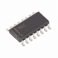
MAX365CSE+ Maxim Integrated Products, MAX365CSE+ Datasheet - Page 7

MAX365CSE+
Manufacturer Part Number
MAX365CSE+
Description
IC SWITCH QUAD SPST 16SOIC
Manufacturer
Maxim Integrated Products
Type
Analog Switchr
Datasheet
1.MAX365CSE.pdf
(13 pages)
Specifications of MAX365CSE+
Function
Switch
Circuit
4 x SPST - NO
On-state Resistance
85 Ohm
Voltage Supply Source
Single, Dual Supply
Voltage - Supply, Single/dual (±)
10 V ~ 30 V, ±4.5 V ~ 20 V
Operating Temperature
0°C ~ 70°C
Mounting Type
Surface Mount
Package / Case
16-SOIC (0.154", 3.90mm Width)
Number Of Switches
Quad
Switch Configuration
SPST
On Resistance (max)
85 Ohms
On Time (max)
250 ns
Off Time (max)
120 ns
Off Isolation (typ)
60 dB
Supply Voltage (max)
+/- 20 V
Supply Voltage (min)
+/- 4.5 V
Supply Current
0.0001 uA
Maximum Power Dissipation
696 mW
Maximum Operating Temperature
+ 70 C
Mounting Style
SMD/SMT
Description/function
Analog Switch
Input Level
CMOS, TTL
Minimum Operating Temperature
0 C
Off State Leakage Current (max)
0.5 nA
Package
16SOIC N
Maximum On Resistance
160@10.8V Ohm
Maximum High Level Output Current
30 mA
Maximum Turn-off Time
200@12V ns
Maximum Turn-on Time
400@12V ns
Switch Architecture
SPST
Power Supply Type
Single|Dual
Lead Free Status / RoHS Status
Lead free / RoHS Compliant
1. Switches are open when power is off.
2. IN_, COM_, NO_, and NC_ should not exceed V+ or
3. Switch leakage is from each analog switch terminal
The main limitation of supply voltages other than ±15V is
reduction in the analog signal range. The MAX364/MAX365
switches operate with ±5V to ±20V bipolar supplies. The
Typical Operating Characteristics graphs show typical on
resistance for ±15V, ±10V, and ±5V supplies. Switching
times increase by a factor of two or more for ±5V opera-
tion. The MAX364/MAX365 operate from unipolar sup-
plies of +10V to +24V. Both parts can be powered from a
single +10V to +24V supply, as well as from unbalanced
supplies, such as +24V and -5V. Connect V- to 0V when
operating with a single supply. VL must be connected to
+5V to be TTL compatible or to V+ for CMOS logic input
levels.
Proper power-supply sequencing is recommended for
all CMOS devices. It is important not to exceed the
absolute maximum ratings, because stresses beyond
those listed may cause permanent damage to the
devices. Always sequence V+ on first, followed by VL,
V-, and logic inputs. If power-supply sequencing is not
possible, protect the devices from overvoltage by
__________Applications Information
V-, even with the power off.
to V+ or V-, not to the other switch terminal.
Operation with Supply Voltages
_______________________________________________________________________________________
Precision, Quad, SPST Analog Switches
Overvoltage Protection
Other than ±15V
Application Hints
O
adding two small signal diodes in series with the supply
pins (Figure 1). Adding the diodes reduces the analog
signal range to 1V below V+ and 1V below V-, but low
switch resistance and low leakage characteristics are
unaffected. Device operation is unchanged, and the
difference between V+ to V- should not exceed +44V.
Figure 1. Overvoltage Protection Using Blocking Diodes
V
g
NO_
V+
V-
COM_
7


