DG211CJ+ Maxim Integrated Products, DG211CJ+ Datasheet - Page 4
DG211CJ+
Manufacturer Part Number
DG211CJ+
Description
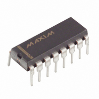
IC SWITCH QUAD SPST 16DIP
Manufacturer
Maxim Integrated Products
Type
Analog Switchr
Datasheet
1.DG211CSE.pdf
(12 pages)
Specifications of DG211CJ+
Function
Switch
Circuit
4 x SPST - NC
On-state Resistance
175 Ohm
Voltage Supply Source
Dual Supply
Voltage - Supply, Single/dual (±)
±4.5 V ~ 18 V
Operating Temperature
0°C ~ 70°C
Mounting Type
Through Hole
Package / Case
16-DIP (0.300", 7.62mm)
Number Of Switches
Quad
Switch Configuration
SPST
On Resistance (max)
175 Ohms
On Time (max)
1000 ns
Off Time (max)
500 ns
Off Isolation (typ)
70 dB
Supply Voltage (max)
+/- 18 V
Supply Voltage (min)
+/- 4.5 V
Supply Current
0.02 mA
Maximum Power Dissipation
842 mW
Maximum Operating Temperature
+ 70 C
Mounting Style
Through Hole
Description/function
Analog Switch
Input Level
CMOS, TTL
Minimum Operating Temperature
0 C
Off State Leakage Current (max)
5 nA
Package
16PDIP N
Maximum On Resistance
175@±15V Ohm
Maximum High Level Output Current
20 mA
Maximum Turn-off Time
500@±15V ns
Maximum Turn-on Time
1000@±15V ns
Switch Architecture
SPST
Power Supply Type
Dual
Lead Free Status / RoHS Status
Lead free / RoHS Compliant


Quad SPST CMOS Analog Switches
ELECTRICAL CHARACTERISTICS (DG201A) (continued)
(V+ = +15V, V- = -15V, GND = 0, T
Note 3: Typical values are for DESIGN AID ONLY, not guaranteed nor subject to production testing.
Note 4: I
4
INPUT
Input Current with Input
Voltage High
Input Current with Input
Voltage Low
DYNAMIC
Turn-ON Time
Turn-OFF Time
Charge Injection
Source OFF-Capacitance
Drain OFF-Capacitance
Channel ON-Capacitance
OFF-Isolation
Crosstalk
(Channel to Channel)
SUPPLY
Positive Supply Current
Negative Supply Current
Power-Supply Range for
Continuous Operation
_______________________________________________________________________________________
D (ON)
PARAMETER
is leakage from driver into “ON” switch.
SYMBOL
+ C
C
C
C
A
t
D (OFF)
S (OFF)
D (ON)
I
OFF1
V
I
t
INH
INL
ON
= +25°C, unless otherwise noted.) (For more information on TYP values see Note 3.)
S (ON)
I +
Q
I -
OP
See Figure 1 Switching Time
Test Circuit
C
R
V
V
V
V
V
V
All channels ON or OFF
All channels ON or OFF
V
V
V
S
IN
D
IN
IN
S
GEN
L
IN
IN
IN
= 0,
= 2.0V, f = 100kHz
= 1000pF, V
= V
= 5V
= 0
= 5V, Z
= 2.4V
= 15V
= 0+
= 0
S
= 0,
CONDITIONS
L
= 75Ω
GEN
f = 140kHz
= 0,
±4.5
MIN
-1.0
-1.0
-0.1
DG201AA
-0.01
TYP
0.02
480
370
20
16
70
90
5
5
MAX
±18
600
450
1.0
0.1
±4.5
MIN
-1.0
-1.0
-0.1
DG201AC, D, E
-0.01
TYP
0.02
480
370
20
16
70
90
5
5
MAX
±18
600
450
1.0
0.1
UNITS
mA
pC
µA
dB
ns
pF
V
Related parts for DG211CJ+
Image
Part Number
Description
Manufacturer
Datasheet
Request
R

Part Number:
Description:
Quad SPST CMOS Analog Switches
Manufacturer:
Maxim Integrated Products
Part Number:
Description:
MAX7528KCWPMaxim Integrated Products [CMOS Dual 8-Bit Buffered Multiplying DACs]
Manufacturer:
Maxim Integrated Products
Datasheet:
Part Number:
Description:
Single +5V, fully integrated, 1.25Gbps laser diode driver.
Manufacturer:
Maxim Integrated Products
Datasheet:
Part Number:
Description:
Single +5V, fully integrated, 155Mbps laser diode driver.
Manufacturer:
Maxim Integrated Products
Datasheet:
Part Number:
Description:
VRD11/VRD10, K8 Rev F 2/3/4-Phase PWM Controllers with Integrated Dual MOSFET Drivers
Manufacturer:
Maxim Integrated Products
Datasheet:
Part Number:
Description:
Highly Integrated Level 2 SMBus Battery Chargers
Manufacturer:
Maxim Integrated Products
Datasheet:
Part Number:
Description:
Current Monitor and Accumulator with Integrated Sense Resistor; ; Temperature Range: -40°C to +85°C
Manufacturer:
Maxim Integrated Products
Part Number:
Description:
TSSOP 14/A�/RS-485 Transceivers with Integrated 100O/120O Termination Resis
Manufacturer:
Maxim Integrated Products
Part Number:
Description:
TSSOP 14/A�/RS-485 Transceivers with Integrated 100O/120O Termination Resis
Manufacturer:
Maxim Integrated Products
Part Number:
Description:
QFN 16/A�/AC-DC and DC-DC Peak-Current-Mode Converters with Integrated Step
Manufacturer:
Maxim Integrated Products
Part Number:
Description:
TDFN/A/65V, 1A, 600KHZ, SYNCHRONOUS STEP-DOWN REGULATOR WITH INTEGRATED SWI
Manufacturer:
Maxim Integrated Products
Part Number:
Description:
Integrated Temperature Controller f
Manufacturer:
Maxim Integrated Products
Part Number:
Description:
SOT23-6/I�/45MHz to 650MHz, Integrated IF VCOs with Differential Output
Manufacturer:
Maxim Integrated Products
Part Number:
Description:
SOT23-6/I�/45MHz to 650MHz, Integrated IF VCOs with Differential Output
Manufacturer:
Maxim Integrated Products
Part Number:
Description:
EVALUATION KIT/2.4GHZ TO 2.5GHZ 802.11G/B RF TRANSCEIVER WITH INTEGRATED PA
Manufacturer:
Maxim Integrated Products