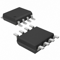
MAX320ESA+ Maxim Integrated Products, MAX320ESA+ Datasheet - Page 5

MAX320ESA+
Manufacturer Part Number
MAX320ESA+
Description
IC SWITCH DUAL SPST 8SOIC
Manufacturer
Maxim Integrated Products
Type
Analog Switchr
Datasheet
1.MAX321CUA.pdf
(8 pages)
Specifications of MAX320ESA+
Function
Switch
Circuit
2 x SPST - NO
On-state Resistance
35 Ohm
Voltage Supply Source
Dual Supply
Voltage - Supply, Single/dual (±)
±3 V ~ 18 V
Current - Supply
1µA
Operating Temperature
-40°C ~ 85°C
Mounting Type
Surface Mount
Package / Case
8-SOIC (0.154", 3.90mm Width)
Package
8SOIC N
Maximum On Resistance
35@±4.5V Ohm
Maximum High Level Output Current
30 mA
Maximum Turn-off Time
100@±5V ns
Maximum Turn-on Time
150@±5V ns
Switch Architecture
SPST
Power Supply Type
Dual
Number Of Switches
Dual
Switch Configuration
SPST
On Resistance (max)
4 Ohms
On Time (max)
150 ns
Off Time (max)
100 ns
Off Isolation (typ)
68 dB
Supply Voltage (max)
+/- 8 V
Supply Voltage (min)
+/- 2.7 V
Supply Current
80 uA
Maximum Power Dissipation
471 mW
Maximum Operating Temperature
+ 85 C
Mounting Style
SMD/SMT
Description/function
Analog Switch
Minimum Operating Temperature
- 40 C
Off State Leakage Current (max)
5 nA
Lead Free Status / RoHS Status
Lead free / RoHS Compliant
Calculate the logic thresholds typically as follows: V
(V+ - 1.5V) and V
Power-supply consumption is minimized when IN1 and
IN2 are driven with logic-high levels equal to V+ and logic-
low levels well below the calculated V
and IN2 can be driven to V- without damage.
Analog signals that range over the entire supply voltage
(V- to V+) can be switched, with very little change in on-
resistance over the entire voltage range (see Typical
Operating Characteristics ). All switches are bidirec-
tional, so NO_, NC_, and COM_ pins can be used as
either inputs or outputs.
Do not exceed the absolute maximum ratings, because
stresses beyond the listed ratings may cause perma-
nent damage to the devices.
Proper power-supply sequencing is recommended for
all CMOS devices. Always apply V+, followed by V-,
before applying analog signals or logic inputs, especial-
ly if the analog or logic signals are not current-limited. If
_____________________Pin Description
__________Applications Information
PIN
2, 6
3, 7
1
4
5
8
(MAX320/MAX322)
(MAX321/MAX322)
COM1, COM2
(MAX321)
(MAX320)
IN2, IN1
NAME
NO2
NO1
NC1
NC2
V+
V-
IL
_______________________________________________________________________________________
= (V+ - 2.5V).
and Overvoltage Protection
Power-Supply Sequencing
Normally Open Analog
Switch Terminal
Normally Closed Analog
Switch Terminal
Analog Switch Common
Terminals
Logic Inputs
Negative Supply
Normally Open Analog
Switch Terminal
Normally Closed Analog
Switch Terminal
Positive Supply
Analog Signal Levels
IL
FUNCTION
of (V+ - 2.5V). IN1
Logic Levels
Precision, Dual-Supply, SPST
IH
=
this sequencing is not possible, and if the analog or
logic inputs are not current-limited to <30mA, add two
small signal diodes (D1, D2) as shown in Figure 1.
Adding protection diodes reduces the analog signal
range to a diode drop (about 0.7V) below V+ for D1,
and a diode drop above V- for D2. Leakage is not
affected by adding the diodes. On-resistance increas-
es by a small amount at low supply voltages. Maximum
supply voltage (V- to V+) must not exceed 17V.
Adding protection diode D1 causes the logic thresh-
olds to be shifted relative to the positive power-supply
rail. This can be significant when low positive supply
voltages (+5V or less) are used. Driving IN1 and IN2 all
the way to the supply rails (i.e., to a diode drop higher
than the V+ pin or a diode drop lower than the V- pin) is
always acceptable.
The protection diodes D1 and D2 also protect against
some overvoltage situations. With the circuit of Figure 1,
if the supply voltage is below the absolute maximum
rating and if a fault voltage up to the absolute maximum
rating is applied to an analog signal pin, no damage
will result. For example, with ±5V supplies, analog sig-
nals up to ±8.5V will not damage the circuit of Figure 1.
If only a single fault signal is present, the fault voltage
can rise to +12V or to -12V without damage.
Figure 1. Overvoltage Protection Using Two External Blocking
Diodes
V g
Analog Switches
NO
POSITIVE SUPPLY
NEGATIVE SUPPLY
V-
V+
D1
D2
COM
MAX320
MAX321
MAX322
5


