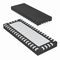
MAX4889BETO+ Maxim Integrated Products, MAX4889BETO+ Datasheet

MAX4889BETO+
Specifications of MAX4889BETO+
Related parts for MAX4889BETO+
MAX4889BETO+ Summary of contents
Page 1
... Supports SAS I, SAS II, and SAS 6.0Gbps (MAX4889C) ♦ Superior Return Loss Better than -10dB (typ) at 5.0GHz ♦ Small 3.5mm x 9.0mm, 42-Pin TQFN Package ♦ Industry-Standard Pinouts Applications PART MAX4889BETO+ MAX4889CETO+ + Denotes a lead(Pb)-free/RoHS-compliant package Exposed pad. Typical Operating Circuit appears at end of data sheet MAX4889B MAX4889C ...
Page 2
PCIe Passive Switches ABSOLUTE MAXIMUM RATINGS (All voltages referenced to GND, unless otherwise noted.) V ...........................................................................-0.3V to +4V CC SEL, _IN_, _OUTA_, _OUTB_ (Note 1) .......-0. Continuous Current (AIN_ to AOUTA_/AOUTB_, BIN_ to BOUTA_/BOUTB_, CIN_ to COUTA_/COUTB_, ...
Page 3
PCIe Passive Switches ELECTRICAL CHARACTERISTICS (continued +3.3V ±10 MIN MAX, noted.) (Note 3) PARAMETER AC PERFORMANCE SEL-to-Switch Turn-On Time SEL-to-Switch Turn-Off Time Propagation Delay Output Skew Between Pairs Output Skew ...
Page 4
PCIe Passive Switches SEL V OUT THE FREQUENCY OF THE SIGNAL SHOULD BE ABOVE THE HIGHPASS FILTER CORNER OF THE COUPLING CAPACITORS. Figure 1. Switching Time 4 _______________________________________________________________________________________ Test Circuits/Timing Diagrams SOURCE MAX4889B/ MAX4889C Z S Σ SEL 50% ...
Page 5
PCIe Passive Switches Σ Σ CALp CALn OUTp OUTn V OUTp V OUTn THE FREQUENCY OF THE SIGNALS SHOULD BE APPROXIMATELY 1/20 OF THE LOWEST DATA RATE. Figure ...
Page 6
PCIe Passive Switches (V = +3.3V +25°C, unless otherwise noted ON-RESISTANCE vs. V _IN_ 8 +3. +3.3V CC 7.5 7.0 6 +3.6V CC 6.0 5.5 5.0 4.5 4.0 ...
Page 7
PCIe Passive Switches AIN+ AIN- BIN+ BIN- CIN+ CIN- DIN+ DIN- _IN_ TO _IN_ TO SEL SEL _OUTA_ _OUTB_ 0 (DEFAULT) ON OFF 1 OFF ON _______________________________________________________________________________________ Functional Diagram/Truth Table MAX4889B AOUTA+ AIN+ AOUTA- AIN- AOUTB+ ...
Page 8
PCIe Passive Switches PIN NAME MAX4889B/ MAX4889C 1 AIN+ Analog Switch 1. Common Positive Terminal. 2 AIN- Analog Switch 1. Common Negative Terminal. 3 AOUTB+ Analog Switch 1. Normally Open Positive Terminal. 4 AOUTB- Analog Switch 1. Normally Open ...
Page 9
PCIe Passive Switches Detailed Description The MAX4889B high-speed passive switch routes PCI Express (PCIe) data or other high-speed signals with amplitude of ≤ 1.2V differential, and common-mode P-P voltage close to 0V between two possible destinations. The MAX4889B is ...
Page 10
PCIe Passive Switches CHANNEL SELECT PCIe NORTH BRIDGE LANE 0 TX LANE 1 TX LANE 2 TX LANE 3 TX CHANNEL SELECT LANE 0 RX LANE 1 RX LANE 2 RX LANE ______________________________________________________________________________________ Typical Operating Circuit: ...
Page 11
PCIe Passive Switches Chip Information PROCESS: CMOS ______________________________________________________________________________________ Package Information For the latest package outline information and land patterns www.maxim-ic.com/packages. Note that a “+”, “#”, or “-” in the package code indicates RoHS status only. Package draw- ...
Page 12
... Maxim cannot assume responsibility for use of any circuitry other than circuitry entirely embodied in a Maxim product. No circuit patent licenses are implied. Maxim reserves the right to change the circuitry and specifications without notice at any time. 12 ____________________Maxim Integrated Products, 120 San Gabriel Drive, Sunnyvale, CA 94086 408-737-7600 © 2010 Maxim Integrated Products ...


