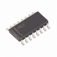
MAX4511ESE+ Maxim Integrated Products, MAX4511ESE+ Datasheet

MAX4511ESE+
Specifications of MAX4511ESE+
Related parts for MAX4511ESE+
MAX4511ESE+ Summary of contents
Page 1
... Ordering Information continued at end of data sheet. *Contact factory for dice specifications. Rail-to-Rail is a registered trademark of Nippon Motorola, Ltd. ________________________________________________________________ Maxim Integrated Products For free samples & the latest literature: http://www.maxim-ic.com, or phone 1-800-998-8800. For small orders, phone 408-737-7600 ext. 3468. SPST Analog Switches o ± ...
Page 2
Quad, Rail-to-Rail, Fault-Protected, SPST Analog Switches ABSOLUTE MAXIMUM RATINGS (Voltages Referenced to GND) V+ ........................................................................-0.3V to +44.0V V- .........................................................................-44.0V to +0. V-................................................................-0.3V to +44.0V COM_, IN_ (Note 1) ..............................(V- - 0.3V) to (V+ + 0.3V) NC_, NO_ (Note ...
Page 3
Quad, Rail-to-Rail, Fault-Protected, ELECTRICAL CHARACTERISTICS—Dual Supplies (continued +15V -15V, GND = 0V PARAMETER FAULT (V+ = +15V -15V, unless otherwise noted.) COM_ Output Leakage Current, Supplies On NO_ or ...
Page 4
Quad, Rail-to-Rail, Fault-Protected, SPST Analog Switches ELECTRICAL CHARACTERISTICS—Dual Supplies (continued +15V -15V, GND = 0V PARAMETER SYMBOL POWER SUPPLY Power-Supply Range V Supply Current V- Supply Current GND Supply ...
Page 5
Quad, Rail-to-Rail, Fault-Protected, ELECTRICAL CHARACTERISTICS—Single +12V Supply (V+ = +10.8V to +13.2V MIN PARAMETER SYMBOL ANALOG SWITCH Fault-Protected Analog V Signal Range Fault-Free Analog Signal Range V Non-Protected Analog Signal Range (COM_ Output) ...
Page 6
Quad, Rail-to-Rail, Fault-Protected, SPST Analog Switches ELECTRICAL CHARACTERISTICS—Single +12V Supply (continued) (V+ = +10.8V to +13.2V MIN PARAMETER SYMBOL LOGIC INPUT IN_ Input Logic Threshold High IN_ Input Logic Threshold Low IN_ Input ...
Page 7
Quad, Rail-to-Rail, Fault-Protected, __________________________________________Typical Operating Characteristics (T = +25°C, unless otherwise noted.) A SWITCH ON-RESISTANCE vs. V (DUAL SUPPLIES) COM 350 V+ = +5V 300 V- = -5V 250 V+ = +12V V+ = +10V V- = -12V V- = ...
Page 8
Quad, Rail-to-Rail, Fault-Protected, SPST Analog Switches (T = +25°C, unless otherwise noted.) A LOGIC-LEVEL THRESHOLD vs. V+ 3.0 2.5 2.0 1.5 1.0 0 (V) Pin Description PIN NAME FUNCTION 1, 16, IN1–IN4 Logic ...
Page 9
Quad, Rail-to-Rail, Fault-Protected, V+ NO_ (NC_) IN_ GND V- -ESD DIODE Figure 1. Block Diagram Overview of MAX4511/MAX4512/MAX4513 The MAX4511/MAX4512/MAX4513 differ considerably from traditional fault-protection switches, with several advantages. First, they are constructed with two paral- lel FETs, allowing very ...
Page 10
Quad, Rail-to-Rail, Fault-Protected, SPST Analog Switches (NO) switch is shown; the normally closed (NC) config- uration is identical except the logic-level translator becomes an inverter. The analog switch is formed by the parallel combination of N-channel FET N1 and P- ...
Page 11
Quad, Rail-to-Rail, Fault-Protected, The MAX4511/MAX4512/MAX4513 operate with bipolar supplies between ±4.5V and ±18V. The V+ and V- sup- plies need not be symmetrical, but their difference can not exceed the absolute maximum rating of 44V. The MAX4511/MAX4512/MAX4513 operate from a ...
Page 12
Quad, Rail-to-Rail, Fault-Protected, SPST Analog Switches IN_ IN_ NO_ OR NC_ 50Ω MAX4511 MAX4512 MAX4513 COM_ GND CONNECTED TO GND (0V) FOR SINGLE-SUPPLY OPERATION. Figure 4. Charge Injection V+ ADDRESS SELECT V- IS ...
Page 13
Quad, Rail-to-Rail, Fault-Protected, V+ 10nF V+ MAX4511 MAX4512 MAX4513 IN_ ADDRESS SELECT NO_, NC_ GND 10nF MEASUREMENTS ARE STANDARDIZED AGAINST SHORT AT SOCKET TERMINALS. OFF ISOLATION IS MEASURED BETWEEN COM_ AND “OFF” NO_ OR NC_ TERMINALS. ON LOSS IS MEASURED ...
Page 14
Quad, Rail-to-Rail, Fault-Protected, SPST Analog Switches Chip Topographies MAX4511 NC1 COM1 IN1 IN2 COM2 V- GND NC4 COM4 IN4 IN3 COM3 0.086" (2.261mm) MAX4512 NO1 COM1 IN1 IN2 COM2 V- GND NO4 COM4 IN4 IN3 COM3 0.086" (2.261mm) TRANSISTOR COUNT: ...
Page 15
Quad, Rail-to-Rail, Fault-Protected, (The package drawing(s) in this data sheet may not reflect the most current specifications. For the latest package outline information www.maxim-ic.com/packages TOP VIEW D e FRONT VIEW ______________________________________________________________________________________ SPST Analog Switches DIM A ...
Page 16
Quad, Rail-to-Rail, Fault-Protected, SPST Analog Switches (The package drawing(s) in this data sheet may not reflect the most current specifications. For the latest package outline information www.maxim-ic.com/packages.) 16 ______________________________________________________________________________________ Package Information (continued) ...
Page 17
... Maxim cannot assume responsibility for use of any circuitry other than circuitry entirely embodied in a Maxim product. No circuit patent licenses are implied. Maxim reserves the right to change the circuitry and specifications without notice at any time. Maxim Integrated Products, 120 San Gabriel Drive, Sunnyvale, CA 94086 408-737-7600______________________17 © 2002 Maxim Integrated Products ...


