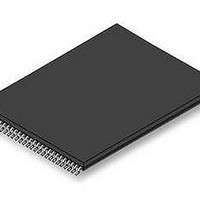
S29GL128S10TFI020 Spansion Inc., S29GL128S10TFI020 Datasheet - Page 12

S29GL128S10TFI020
Manufacturer Part Number
S29GL128S10TFI020
Description
Flash 128 MBIT 3V 100NS PAGE MODE FLASH
Manufacturer
Spansion Inc.
Datasheet
1.S29GL128S10TFI020.pdf
(97 pages)
Specifications of S29GL128S10TFI020
Data Bus Width
16 bit
Memory Type
Flash
Memory Size
128 Mbit
Architecture
Uniform
Timing Type
Asynchronous
Interface Type
CFI
Access Time
100 ns
Supply Voltage (max)
3.6 V
Supply Voltage (min)
2.7 V
Maximum Operating Current
100 mA
Operating Temperature
- 40 C to + 85 C
Mounting Style
SMD/SMT
Package / Case
TSOP-56
Lead Free Status / Rohs Status
Compliant
Available stocks
Company
Part Number
Manufacturer
Quantity
Price
Company:
Part Number:
S29GL128S10TFI020
Manufacturer:
SPANSION
Quantity:
101
Company:
Part Number:
S29GL128S10TFI020
Manufacturer:
SPANSION
Quantity:
1 001
Part Number:
S29GL128S10TFI020
Manufacturer:
SPANSION
Quantity:
20 000
Software Interface
2. Address Space Maps
12
There are several separate address spaces that may appear within the address range of the flash memory
device. One address space is visible (entered) at any given time.
Flash Memory Array: the main non-volatile memory array used for storage of data that may be randomly
ID/CFI: a Flash memory array used for Spansion factory programmed device characteristics information.
Secure Silicon Region (SSR): a One Time Programmable (OTP) non-volatile memory array used for
Lock Register: an OTP non-volatile word used to configure the ASP features and lock the SSR.
Persistent Protection Bits (PPB): a non-volatile flash memory array with one bit for each Sector. When
PPB Lock: a volatile register bit used to enable or disable programming and erase of the PPB bits.
Password: an OTP non-volatile array used to store a 64-bit password used to enable changing the state of
Dynamic Protection Bits (DYB): a volatile array with one bit for each Sector. When set, each bit protects the
Status Register: a volatile register used to display Embedded Algorithm status.
Data Polling Status: a volatile register used as an alternate, legacy software compatible, way to display
ECC Status: provides the status of any error detection or correction action taken when reading the selected
The main Flash Memory Array is the primary and default address space but, it may be overlaid by one other
address space, at any one time. Each alternate address space is called an Address Space Overlay (ASO).
Each ASO replaces (overlays) the entire flash device address range. Any address range not defined by a
particular ASO address map, is reserved for future use. All read accesses outside of an ASO address map
returns non-valid (undefined) data. The locations will display actively driven data but the meaning of whatever
1’s or 0’s appear are not defined.
There are four address map modes that determine what appears in the flash device address space at any
given time:
Read Mode
Data Polling Mode
Status Register (SR) Mode
Address Space Overlay (ASO) Mode
In Read Mode the entire Flash Memory Array may be directly read by the host system memory controller. The
memory device Embedded Algorithm Controller (EAC), puts the device in Read mode during Power-on, after
a Hardware Reset, after a Command Reset, or after an Embedded Algorithm (EA) is suspended. Read
accesses and commands are accepted in read mode. A subset of commands are accepted in read mode
when an EA is suspended.
While in any mode, the Status Register read command may be issued to cause the Status Register ASO to
appear at every word address in the device address space. In this Status Register ASO Mode, the device
interface waits for a read access and, any write access is ignored. The next read access to the device
accesses the content of the status register, exits the Status Register ASO, and returns to the previous
(calling) mode in which the Status Register read command was received.
In EA mode the EAC is performing an Embedded Algorithm, such as programming or erasing a non-volatile
memory array. While in EA mode, none of the main Flash Memory Array is readable because the entire flash
accessed by asynchronous read operations.
This area contains the Device Identification (ID) and Common Flash Interface (CFI) information tables.
Spansion factory programmed permanent data, and customer programmable permanent data.
programmed, each bit protects the related Sector from erasure and programming.
the PPB Lock Bit when using Password Mode sector protection.
related Sector from erasure and programming.
Embedded Algorithm status.
Page.
D a t a
S h e e t
GL-S MirrorBit
( A d v a n c e
®
Family
I n f o r m a t i o n )
S29GL_128S_01GS_00_01 February 11, 2011


