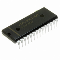
DG506ACJ+ Maxim Integrated Products, DG506ACJ+ Datasheet - Page 2

DG506ACJ+
Manufacturer Part Number
DG506ACJ+
Description
IC MULTIPLEXER 16X1 28DIP
Manufacturer
Maxim Integrated Products
Datasheet
1.DG506ACJ.pdf
(7 pages)
Specifications of DG506ACJ+
Function
Multiplexer
Circuit
1 x 16:1
On-state Resistance
400 Ohm
Voltage Supply Source
Dual Supply
Voltage - Supply, Single/dual (±)
±4.5 V ~ 18 V
Operating Temperature
0°C ~ 70°C
Mounting Type
Through Hole
Package / Case
28-DIP (0.600", 15.24mm)
Lead Free Status / RoHS Status
Lead free / RoHS Compliant
Monolithic CMOS Analog Multiplexers
ABSOLUTE MAXIMUM RATINGS
(Voltages referenced to V
V
GND .......................................................................................25V
Digital Inputs V
Current, Any Terminal Except S or D .................................30mA
Continuous Current, S or D ................................................20mA
Peak Current, S or D (pulsed at 1ms, 10% duty cycle max) ... 40mA
*All leads soldered or welded to PCB.
ELECTRICAL CHARACTERISTICS
(V+ = 15V, V- = -15V, V
2
Stresses beyond those listed under “Absolute Maximum Ratings” may cause permanent damage to the device. These are stress ratings only, and functional
operation of the device at these or any other conditions beyond those indicated in the operational sections of the specifications is not implied. Exposure to absolute
maximum rating conditions for extended periods may affect device reliability.
+
SWITCH
Analog Signal
Range
Drain-to-
Source
On-Resistance
Greatest
Change in
Drain-Source
On-Resistance
Between
Channels
Source Off-
Leakage
Current
Drain Off-
Leakage
Current
PARAMETER
..........................................................................................44V
S
, V
D
SYMBOL
V
R
R
I
I
ANALOG
(Note 1) .......................-2V to (V
D(OFF)
DS(ON)
DS(ON)
S(OFF)
GND
-
.)
= 0V, T
Sequence each
switch on,
V
V
V
-10V P V
V
V
DG506A,
V
V
DG507A,
V
V
∆
AL
AH
EN
EN
AL
EN
AL
EN
AL
R
20mA, whichever occurs first
DS(ON)
A
= 0.8V,
= 0.8V
= 0.8V
= 0.8V
= 2.4V
= 0.8V,
= 0.8V,
= 0.8V,
= 2.4V,
= +25NC, unless otherwise indicated.)
=
S
CONDITIONS
P +10V
R
DS(ON)MAX
R
DS(ON)AVE
V
I
V
I
V
V
V
V
V
V
V
V
V
V
V
V
S
S
−
+
D
D
S
D
S
D
D
S
D
S
D
S
D
S
R
= -200FA
= -200FA
DS(ON)MIN
= 10V,
= -10V,
= -10V
= 10V
= -10V
= 10V
+ 2V) or
= 10V,
= -10V,
= -10V
= 10V
= 10V,
= -10V,
= 10V,
= -10V,
(Note 2)
MIN
-15
-10
-10
Continuous Power Dissipation (T
Operating Temperature Range (A Suffix) ........ -55NC to +125NC
Storage Temperature (A and B Suffix) ............. -65NC to +150NC
Lead Temperature (soldering, 10s) ................................+300NC
-1
-1
-5
-5
28-Pin Ceramic DIP (derate 16.7mW/NC above +70NC) ..1333mW
28-Pin Plastic DIP (derate 14.3mW/NC above +70NC) ...1143mW
28-Pin Wide SO (derate 12.5mW/°C above +70°C) ..1000mW
DG506AA
DG507AA
(Note 3)
-0.005
-0.015
0.002
0.007
-0.03
TYP
0.02
270
230
6
MAX
+15
+10
+10
400
400
+1
+1
+5
+5
(C Suffix) ....................... -65NC to +125NC
(Note 2)
MIN
-15
-20
-20
-10
-10
-5
-5
(B Suffix) .......... -25NC to +85NC
(C Suffix) ................ 0NC to +70N
DG506AB/C
DG507AB/C
A
(Note 3)
= +70°C)*
-0.005
-0.015
0.002
0.007
-0.03
TYP
0.02
270
230
6
MAX
+15
+20
+20
+10
+10
450
450
+5
+5
UNITS
nA
nA
%
I
V


