MC14016BCPG ON Semiconductor, MC14016BCPG Datasheet
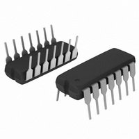
IC SWITCH 1X1 14DIP

MC14016BCPG

Manufacturer Part Number
MC14016BCPG
Description
IC SWITCH 1X1 14DIP
Manufacturer
ON Semiconductor
Series
4000Br
Datasheets

Specifications of MC14016BCPG

Function
Switch
Circuit
1 x 1:1
On-state Resistance
400 Ohm
Voltage Supply Source
Single Supply
Voltage - Supply, Single/dual (±)
3 V ~ 18 V
Current - Supply
0.0015µA
Operating Temperature
-55°C ~ 125°C
Mounting Type
Through Hole
Package / Case
14-DIP (0.300", 7.62mm)
Switch Configuration
SPST
On Resistance (max)
660 Ohms
On Time (max)
45 ns
Off Time (max)
90 ns
Supply Voltage (max)
18 V
Supply Voltage (min)
3 V
Maximum Power Dissipation
500 mW
Maximum Operating Temperature
+ 125 C
Mounting Style
Through Hole
Minimum Operating Temperature
- 55 C
Propagation Delay Time
45 ns
Lead Free Status / RoHS Status
Lead free / RoHS Compliant
Other names
MC14016BCPGOS
MC14016B
Quad Analog Switch/
Quad Multiplexer
P−channel and N−channel enhancement mode devices in a single
monolithic structure. Each MC14016B consists of four independent
switches capable of controlling either digital or analog signals. The
quad bilateral switch is used in signal gating, chopper, modulator,
demodulator and CMOS logic implementation.
Features
Stresses exceeding Maximum Ratings may damage the device. Maximum
Ratings are stress ratings only. Functional operation above the Recommended
Operating Conditions is not implied. Extended exposure to stresses above the
Recommended Operating Conditions may affect device reliability.
1. Temperature Derating:
static voltages or electric fields. However, precautions must be taken to avoid
applications of any voltage higher than maximum rated voltages to this
high−impedance circuit. For proper operation, V
to the range V
(e.g., either V
MAXIMUM RATINGS
© Semiconductor Components Industries, LLC, 2009
September, 2009 − Rev. 8
Symbol
V
The MC14016B quad bilateral switch is constructed with MOS
in
This device contains protection circuitry to guard against damage due to high
Unused inputs must always be tied to an appropriate logic voltage level
transfer characteristic design causes more parasitic coupling
capacitance than CD4016)
The MC14066B
Protection. Antistatic Precautions Must Be Taken.
Diode Protection on All Inputs
Supply Voltage Range = 3.0 Vdc to 18 Vdc
Linearized Transfer Characteristics
Low Noise − 12 nV/√Cycle, f ≥ 1.0 kHz typical
Pin−for−Pin Replacements for CD4016B, CD4066B (Note improved
For Lower R
This Device Has Inputs and Outputs Which Do Not Have ESD
These are Pb−Free Devices
V
I
T
Plastic “P and D/DW” Packages: – 7.0 mW/_C From 65_C To 125_C
P
, V
SW
T
T
I
DD
stg
in
D
A
L
out
DC Supply Voltage Range
Input or Output Voltage Range
(DC or Transient)
Input Current (DC or Transient)
per Control Pin
Switch Through Current
Power Dissipation, per Package
(Note 1)
Ambient Temperature Range
Storage Temperature Range
Lead Temperature
(8−Second Soldering)
SS
SS
or V
v (V
ON
DD
, Use The HC4016 High−Speed CMOS Device or
in
). Unused outputs must be left open.
Parameter
or V
(Voltages Referenced to V
out
) v V
DD
.
in
and V
−0.5 to V
SS
−0.5 to +18.0
−55 to +125
−65 to +150
out
)
Value
± 10
± 25
should be constrained
500
260
DD
+ 0.5
1
Unit
mW
mA
mA
°C
°C
°C
V
V
See detailed ordering and shipping information in the package
dimensions section on page 2 of this data sheet.
ORDERING INFORMATION
A
WL, L
YY, Y
WW, W
G
http://onsemi.com
CASE 751A
SOEIAJ−14
CASE 646
CASE 965
P SUFFIX
D SUFFIX
F SUFFIX
PDIP−14
SOIC−14
= Wafer Lot
= Assembly Location
= Year
= Work Week
= Pb−Free Indicator
Publication Order Number:
14
1
14
14
1
1
MC14016BCP
DIAGRAMS
AWLYYWWG
MARKING
MC14016B
AWLYWW
MC14016B/D
ALYWG
14016BG

Related parts for MC14016BCPG

MC14016BCPG Summary of contents

Page 1

MC14016B Quad Analog Switch/ Quad Multiplexer The MC14016B quad bilateral switch is constructed with MOS P−channel and N−channel enhancement mode devices in a single monolithic structure. Each MC14016B consists of four independent switches capable of controlling either digital or analog ...

Page 2

... LOGIC DIAGRAM RESTRICTIONS ≤ V ≤ ≤ V ≤ out DD ORDERING INFORMATION Device MC14016BCPG MC14016BDG MC14016BDR2G MC14016BFELG †For information on tape and reel specifications, including part orientation and tape sizes, please refer to our Tape and Reel Packaging Specifications Brochure, BRD8011/ CONTROL 1 13 CONTROL 1 12 CONTROL 4 CONTROL 2 ...

Page 3

ELECTRICAL CHARACTERISTICS Î Î Î Î Î ...

Page 4

ELECTRICAL CHARACTERISTICS Î Î Î Î Î ...

Page 5

raised from When out TO ALL 4 CIRCUITS PULSE CONTROL GENERATOR INPUT f c ...

Page 6

V out Figure 5. R Characteristics ON Test Circuit V out 90 PZH PHZ ...

Page 7

AND 100 2 4 3.0 ...

Page 8

Figure A illustrates use of the Analog Switch. The 0−to−5 V Digital Control signal is used to directly control analog signal. The digital control logic levels are determined by V and V . The V voltage is ...

Page 9

−T− SEATING PLANE 0.13 (0.005) PACKAGE DIMENSIONS PDIP−14 CASE 646−06 ISSUE http://onsemi.com 9 NOTES: 1. DIMENSIONING AND TOLERANCING PER ANSI ...

Page 10

... G −T− SEATING 14 PL PLANE 0.25 (0.010 14X 0.58 *For additional information on our Pb−Free strategy and soldering details, please download the ON Semiconductor Soldering and Mounting Techniques Reference Manual, SOLDERRM/D. PACKAGE DIMENSIONS SOIC−14 CASE 751A−03 ISSUE 0.25 (0.010 ...

Page 11

... Opportunity/Affirmative Action Employer. This literature is subject to all applicable copyright laws and is not for resale in any manner. PUBLICATION ORDERING INFORMATION LITERATURE FULFILLMENT: Literature Distribution Center for ON Semiconductor P.O. Box 5163, Denver, Colorado 80217 USA Phone: 303−675−2175 or 800−344−3860 Toll Free USA/Canada Fax: 303− ...

Related keywords