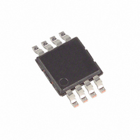
MAX4731EUA+ Maxim Integrated Products, MAX4731EUA+ Datasheet

MAX4731EUA+
Specifications of MAX4731EUA+
Related parts for MAX4731EUA+
MAX4731EUA+ Summary of contents
Page 1
... PC board area. Battery-Powered Systems Audio/Video-Signal Routing Low-Voltage Data-Acquisition Systems Cell Phones Communications Circuits PDAs UCSP is a trademark of Maxim Integrated Products, Inc. µMAX is a registered trademark of Maxim Integrated Products, Inc. Pin Configurations/Functional Diagrams/Truth Tables TOP VIEW MAX4731 (BUMPS COM1 ON BOTTOM) NO1 ...
Page 2
Dual SPST Analog Switches in UCSP ABSOLUTE MAXIMUM RATINGS (All voltages referenced to GND.) V+ ...........................................................................-0.3V to +12V IN_, COM_, NO_, NC_ (Note 1)....................-0.3V to (V+ + 0.3V) Continuous Current (any pin) ...........................................±10mA Peak Current (any pin, pulsed at ...
Page 3
Dual SPST Analog Switches in UCSP ELECTRICAL CHARACTERISTICS—Single +3V Supply (continued) (V+ = +3V ±10 +2.0V +0.8V (Notes 3, 4) PARAMETER SYMBOL DYNAMIC CHARACTERISTICS Turn-On Time Turn-Off Time Break-Before-Make (MAX4733 Only, Note ...
Page 4
Dual SPST Analog Switches in UCSP ELECTRICAL CHARACTERISTICS—Single +5V Supply (V+ = +5V ±10 +2.0V +0.8V (Notes 3, 4) PARAMETER SYMBOL ANALOG SWITCH V COM_ Analog Signal Range V NO_ On-Resistance R ...
Page 5
Dual SPST Analog Switches in UCSP ELECTRICAL CHARACTERISTICS—Single +5V Supply (V+ = +5V ±10 +2.0V +0.8V (Notes 3, 4) PARAMETER SYMBOL Crosstalk (Note 10) NO_ or NC_ Off-Capacitance COM_ Off-Capacitance C COM_(OFF) ...
Page 6
Dual SPST Analog Switches in UCSP (T = +25°C, unless otherwise noted.) A ON-RESISTANCE vs. V COM +2. +3. +5. +10. ...
Page 7
Dual SPST Analog Switches in UCSP (T = +25°C, unless otherwise noted.) A TURN-ON/OFF TIME vs. TEMPERATURE +3. +5. ...
Page 8
Dual SPST Analog Switches in UCSP Analog Signal Levels Analog signals that range over the entire supply voltage (GND to V+) pass with very little change in R Typical Operating Characteristics). The bidirectional switches allow NO_, NC_, and COM_ ...
Page 9
Dual SPST Analog Switches in UCSP MAX4731 MAX4732 MAX4733 NO_ OR NC_ V N_ IN_ GND LOGIC INPUT C INCLUDES FIXTURE AND STRAY CAPACITANCE OUT ...
Page 10
Dual SPST Analog Switches in UCSP V+ 10nF SIGNAL V+ GENERATOR 0dBm COM_ NC_ ANALYZER OR NO_ GND R L 10nF V- NOTE: DUAL SUPPLIES USED TO ACCOMODATE GROUND-REFERENCED INSTRUMENTS. Figure 5. Off-Isolation/On-Channel Bandwidth V+ 10nF V+ COM_ CAPACITANCE ...
Page 11
Dual SPST Analog Switches in UCSP Pin Configurations/Functional Diagrams/Truth Tables (continued) TOP VIEW MAX4733 (BUMPS COM1 ON BOTTOM NO1 IN1 COM2 UCSP TOP VIEW MAX4731 NO1 COM1 2 7 IN1 ...
Page 12
Dual SPST Analog Switches in UCSP (The package drawing(s) in this data sheet may not reflect the most current specifications. For the latest package outline information go to www.maxim-ic.com/packages.) 12 ______________________________________________________________________________________ Package Information PACKAGE OUTLINE, 3x3 UCSP 1 21-0093 ...
Page 13
Dual SPST Analog Switches in UCSP (The package drawing(s) in this data sheet may not reflect the most current specifications. For the latest package outline information go to www.maxim-ic.com/packages.) COMMON DIMENSIONS SYMBOL MIN. A 0.70 D 2.90 E 2.90 ...
Page 14
... Maxim cannot assume responsibility for use of any circuitry other than circuitry entirely embodied in a Maxim product. No circuit patent licenses are implied. Maxim reserves the right to change the circuitry and specifications without notice at any time. 14 ____________________Maxim Integrated Products, 120 San Gabriel Drive, Sunnyvale, CA 94086 408-737-7600 © 2006 Maxim Integrated Products Package Information (continued) ...


