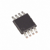
MAX4641EUA+ Maxim Integrated Products, MAX4641EUA+ Datasheet - Page 2

MAX4641EUA+
Manufacturer Part Number
MAX4641EUA+
Description
IC SWITCH DUAL SPST 8UMAX
Manufacturer
Maxim Integrated Products
Datasheet
1.MAX4641EUA.pdf
(10 pages)
Specifications of MAX4641EUA+
Function
Switch
Circuit
2 x SPST - NO
On-state Resistance
4 Ohm
Voltage Supply Source
Single Supply
Voltage - Supply, Single/dual (±)
1.8 V ~ 5.5 V
Current - Supply
1µA
Operating Temperature
-40°C ~ 85°C
Mounting Type
Surface Mount
Package / Case
8-TSSOP, 8-MSOP (0.118", 3.00mm Width)
Number Of Switches
Dual
Switch Configuration
SPDT
On Resistance (max)
4 Ohms
On Time (max)
15 ns
Off Time (max)
8 ns
Off Isolation (typ)
- 80 dB
Supply Voltage (max)
5.5 V
Supply Voltage (min)
1.8 V
Supply Current
0.001 uA
Maximum Power Dissipation
362 mW
Maximum Operating Temperature
+ 85 C
Mounting Style
SMD/SMT
Description/function
Analog Switch
Input Level
CMOS, TTL
Minimum Operating Temperature
- 40 C
Off State Leakage Current (max)
0.25 nA
Lead Free Status / RoHS Status
Lead free / RoHS Compliant
ABSOLUTE MAXIMUM RATINGS
(All Voltages Referenced to GND)
V+ .............................................................................-0.3V to +6V
IN_, COM_, NO_, NC_ (Note 1)....................-0.3V to (V+ + 0.3V)
Continuous Current (any terminal)....................................±20mA
Continuous Current (NO_, NC_, COM_)...........................±50mA
Peak Current (NO_, NC_, COM_, pulsed at 1ms,
High-Speed, Low-Voltage, 4Ω, Dual SPST
CMOS Analog Switches
Note 1: Signals on NO_, NC_, COM_, or IN_ exceeding V+ or GND are clamped by internal diodes. Limit forward-diode current to
Stresses beyond those listed under “Absolute Maximum Ratings” may cause permanent damage to the device. These are stress ratings only, and functional
operation of the device at these or any other conditions beyond those indicated in the operational sections of the specifications is not implied. Exposure to
absolute maximum rating conditions for extended periods may affect device reliability.
ELECTRICAL CHARACTERISTICS—Single +5V Supply
(V+ = +4.5V to +5.5V, V
2
ANALOG SWITCH
DIGITAL INPUTS
Analog Signal Range
On-Resistance
On-Resistance Match
Between Channels
(Notes 2, 8)
On-Resistance Flatness
(Note 3)
NO_, NC_ Off-Leakage
Current (Note 4)
COM_ Off-Leakage Current
(Note 4)
COM_ On-Leakage Current
(Notes 4, 5)
DIGITAL INPUTS
IN_ Input Logic High
IN_ Input Logic Low
IN_ Input Current
10% duty cycle)........................................................ ±100mA
_______________________________________________________________________________________
maximum current rating.
PARAMETER
INH
= 2.4V, V
I
I
I
I
NO_(OFF)
NC_(OFF)
COM_(OFF)
SYMBOL
COM_(ON)
V
V
∆R
R
V
COM_
R
INL
NO_
V
FLAT
V
I
NC_
ON
IN
IH
IL
ON
= 0.8V, T
,
,
,
V+ = 4.5V,
I
or V
V+ = 4.5V, I
10mA, V
V
V+ = 4.5V, I
10mA, V
V
V+ = 5.5V, V
1V or 4.5V, V
V
V+ = 5.5V, V
1V or 4.5V, V
V
V+ = 5.5V, V
1V or 4.5V
V
COM_
NC_
NC_
NC_
NC_
IN_
A
NC_
= T
= 0.8V or 2.4V
= 0 to V+
= 0 to V+
= 4.5V or 1V
= 4.5V or 1V
= 10mA, V
MIN
= 0 to V+
NO_
NO_
to T
COM_
COM_
COM_
COM_
COM_
or
or
NO_
NO_
MAX
CONDITIONS
NO_
or
or
=
=
=
=
=
, unless otherwise noted. Typical values are at T
Continuous Power Dissipation (T
Operating Temperature Range ...........................-40°C to +85°C
Junction Temperature ......................................................+150°C
Storage Temperature Range .............................-65°C to +150°C
Lead Temperature (soldering, 10s) ................................ +300°C
T
T
T
T
T
T
T
T
T
T
T
T
8-Pin µMAX (derate 4.5mW/°C above +70°C) ........... 362mW
8-Pin QFN (derate 24.4mW/°C above +70°C) ......... 1951mW
A
A
A
A
A
A
A
A
A
A
A
A
= +25°C
= T
= +25°C
= T
= +25°C
= T
= +25°C
= T
= +25°C
= T
= +25°C
= T
MIN
MIN
MIN
MIN
MIN
MIN
to T
to T
to T
to T
to T
to T
MAX
MAX
MAX
MAX
MAX
MAX
-0.25
-0.35
-0.25
-0.35
-0.25
-0.35
MIN
-0.1
2.4
0
A
= +70°C)
0.005
TYP
0.85
0.01
0.01
0.01
2.5
0.2
A
MAX
0.25
0.35
0.25
0.35
0.25
0.35
= +25°C.)
V+
0.6
0.8
1.5
0.8
0.1
4
5
1
UNITS
nA
nA
nA
µA
Ω
Ω
Ω
V
V
V


