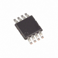
MAX4722EUA+ Maxim Integrated Products, MAX4722EUA+ Datasheet - Page 9

MAX4722EUA+
Manufacturer Part Number
MAX4722EUA+
Description
IC SWITCH DUAL SPST 8UMAX
Manufacturer
Maxim Integrated Products
Datasheet
1.MAX4721EUA.pdf
(14 pages)
Specifications of MAX4722EUA+
Function
Switch
Circuit
2 x SPST - NC
On-state Resistance
4.5 Ohm
Voltage Supply Source
Single Supply
Voltage - Supply, Single/dual (±)
1.8 V ~ 5.5 V
Current - Supply
1µA
Operating Temperature
-40°C ~ 85°C
Mounting Type
Surface Mount
Package / Case
8-TSSOP, 8-MSOP (0.118", 3.00mm Width)
Lead Free Status / RoHS Status
Lead free / RoHS Compliant
Power-supply bypassing improves noise margin and
prevents switching noise from propagating from the V+
supply to other components. A 0.1µF capacitor connect-
ed from V+ to GND is adequate for most applications.
Caution: Do not exceed the absolute maximum rat-
ings because stresses beyond the listed ratings may
cause permanent damage to the device.
For general UCSP package information and PC layout
considerations, please refer to the Maxim Application
Note (Wafer-Level Chip-Scale Package).
Figure 1. Switching Time
Figure 2. Break-Before-Make Interval
LOGIC
INPUT
MAX4721/
MAX4722/
MAX4723
MAX4723
V
V
COM1
COM2
LOGIC
INPUT
V
COM1
COM2
IN_
4.5
N_
UCSP Package Considerations
_______________________________________________________________________________________
and Overvoltage Protection
NO_
OR NC_
IN_
GND
GND
Power-Supply Sequencing
Power-Supply Bypassing
V+
V+
C
C
V
L
Dual SPST Analog Switches in UCSP
L
OUT
INCLUDES FIXTURE AND STRAY CAPACITANCE.
INCLUDES FIXTURE AND STRAY CAPACITANCE.
NO_
NC_
= V
COM
V+
V+
COM_
(
R
L
- R
R
R
L
L2
ON
)
R
V
OUT2
L
C
L2
C
R
L
L1
V
OUT
V
OUT1
C
L1
The chip-scale package (UCSP) represents a unique
packaging form factor that may not perform equally to a
packaged product through traditional mechanical relia-
bility tests. UCSP reliability is integrally linked to the
user’s assembly methods, circuit board material, and
usage environment. The user should closely review
these areas when considering use of a UCSP package.
Performance through Operating Life Test and Moisture
Resistance remains uncompromised as it is primarily
determined by the wafer-fabrication process.
Mechanical stress performance is a greater considera-
tion for a UCSP package. UCSPs are attached through
direct solder contact to the user’s PC board, foregoing
the inherent stress relief of a packaged product lead
frame. Solder joint contact integrity must be consid-
ered. Information on Maxim’s qualification plan, test
data, and recommendations are detailed in the UCSP
application note, which can be found on Maxim’s web-
site at www.maxim-ic.com.
OUTPUT
SWITCH
OUTPUT 1
OUTPUT 2
LOGIC
INPUT
SWITCH
SWITCH
(V
(V
LOGIC
INPUT
OUT1
OUT2
Test Circuits/Timing Diagrams
)
)
V
V
0V
IH
IL
V
V
0V
0V
IH
IL
LOGIC INPUT WAVEFORMS INVERTED FOR SWITCHES
THAT HAVE THE OPPOSITE LOGIC SENSE.
t
50%
D
V
t
50%
ON
OUT
0.9 x V
0.9 x V
0UT1
0UT
UCSP Reliability
t
D
t
OFF
0.9 x V
0.9 x V
OUT2
OUT
9


