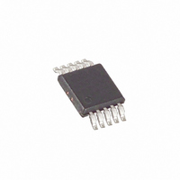
MAX4695EUB+ Maxim Integrated Products, MAX4695EUB+ Datasheet - Page 7

MAX4695EUB+
Manufacturer Part Number
MAX4695EUB+
Description
IC SWITCH DUAL SPDT 10UMAX
Manufacturer
Maxim Integrated Products
Datasheet
1.MAX4695EUB.pdf
(11 pages)
Specifications of MAX4695EUB+
Function
Switch
Circuit
2 x SPDT
On-state Resistance
60 Ohm
Voltage Supply Source
Single Supply
Voltage - Supply, Single/dual (±)
1.8 V ~ 5.5 V
Current - Supply
1µA
Operating Temperature
-40°C ~ 85°C
Mounting Type
Surface Mount
Package / Case
10-MSOP, Micro10™, 10-uMAX, 10-uSOP
Lead Free Status / RoHS Status
Lead free / RoHS Compliant
The MAX4695 is a low-voltage, dual single-pole/dou-
ble-throw (SPDT) analog switch that operates from a
single +1.8V to +5.5V supply. When powered from a
+2.7V supply, the device has a 60
tance (R
(max) R
logic compatible from a +2.7V to +3.3V supply.
The MAX4695 logic inputs are 1.8V CMOS logic com-
patible for 3V operation and TTL compatible for 5V
operation of V+. Driving IN_ rail-to-rail minimizes power
consumption.
Analog signals that range over the entire supply volt-
age (V+ to GND) are passed with very little change in
on-resistance (see Typical Operating Characteristics).
The switches are bidirectional, so the NO_, NC_, and
COM_ pins can be either inputs or outputs.
Caution: Do not exceed the absolute maximum rat-
ings because stresses beyond the listed ratings
may cause permanent damage to devices.
Proper power-supply sequencing is recommended for
all CMOS devices. Always apply V+ before applying
analog signals, especially if the analog signal is not
current limited. If this sequencing is not possible, and if
the analog inputs are not current limited to <20mA, add
µMAX
10
—
1
2
3
4
5
6
7
8
9
ON
ON
), with 3
flatness. The digital logic inputs are 1.8V-
PIN
Applications Information
Power-Supply Sequencing and
_______________________________________________________________________________________
TQFN
6, 10
12
11
Detailed Description
1
2
3
4
5
7
8
9
(max) R
Overvoltage Protection
Digital Control Inputs
Analog Signal Levels
ON
NAME
COM2
COM1
GND
NO1
NO2
N.C.
NC2
NC1
IN1
IN2
V+
matching and 10
SPDT Analog Switch in Thin QFN
(max) on-resis-
Digital Control Input Switch 1
Analog Switch 1—Normally Open Terminal
Ground
Analog Switch 2—Normally Open Terminal
Digital Control Input Switch 2
Analog Switch 2—Common Terminal
No Connection. Not internally connected.
Analog Switch 2—Normally Closed Terminal
Positive Supply Voltage Input
Analog Switch 1—Normally Closed Terminal
Analog Common Switch 1
a small signal diode (D1) as shown in Figure 1. If the
analog signal can dip below GND, add D2. Adding
protection diodes reduces the analog range to a diode
drop (about 0.7V) below V+ (for D1), and a diode drop
above ground (for D2). On-resistance increases slightly
at low supply voltages. Maximum supply voltage (V+)
must not exceed +6V.
Adding protection diode D2 causes the logic threshold
to be shifted relative to GND. TTL compatibility is not
guaranteed when D2 is added.
Protection diodes D1 and D2 also protect against some
overvoltage situations. In the circuit in Figure 1, if the
supply voltage is below the absolute maximum rating,
and if a fault voltage up to the absolute maximum rating
is applied to an analog signal pin, no damage will result.
Figure 1. Overvoltage Protection Using Two External Blocking
Diodes
Low-Voltage, 60
V g
FUNCTION
NO
POSITIVE SUPPLY
GND
V+
D1
D2
Pin Description
COM
MAX4695
Dual
7


