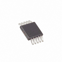
MAX4704EUB+ Maxim Integrated Products, MAX4704EUB+ Datasheet - Page 2

MAX4704EUB+
Manufacturer Part Number
MAX4704EUB+
Description
IC MULTIPLEXER 4X1 10UMAX
Manufacturer
Maxim Integrated Products
Datasheet
1.MAX4704EUB.pdf
(11 pages)
Specifications of MAX4704EUB+
Function
Multiplexer
Circuit
1 x 4:1
On-state Resistance
60 Ohm
Voltage Supply Source
Single Supply
Voltage - Supply, Single/dual (±)
1.8 V ~ 5.5 V
Current - Supply
1µA
Operating Temperature
-40°C ~ 85°C
Mounting Type
Surface Mount
Package / Case
10-MSOP, Micro10™, 10-uMAX, 10-uSOP
Lead Free Status / RoHS Status
Lead free / RoHS Compliant
Low-Voltage, 60 Ω ,
4:1 Analog Multiplexer in QFN
ABSOLUTE MAXIMUM RATINGS
(Voltages Referenced to GND)
V+ .............................................................................-0.3V to +6V
All Other Pins (Note 1)................................ -0.3V to (V+ + 0.3V)
Continuous Current COM, NO_ ........................................±20mA
Peak Current COM, NO_
ESD per Method 3015.7.......................................................>2kV
ELECTRICAL CHARACTERISTICS—Single +3V Supply
(V+ = +2.7V to +3.3V, V
T
Note 1: Signals on INH, ADD_, NO_, and COM exceeding V+ or GND are clamped by internal diodes. Limit forward-diode current to
Stresses beyond those listed under “Absolute Maximum Ratings” may cause permanent damage to the device. These are stress ratings only, and functional
operation of the device at these or any other conditions beyond those indicated in the operational sections of the specifications is not implied. Exposure to
absolute maximum rating conditions for extended periods may affect device reliability.
2
A
ANALOG SWITCH
Analog Signal Range
On-Resistance Match
Between Channels (Note 4)
On-Resistance Flatness
(Note 5)
NO_ Off-Leakage
Current (Note 6)
COM On-Leakage Current
(Note 6)
COM Off-Leakage Current
(Note 6)
DYNAMIC
Address Transition Time
Inhibit Turn-On Time
Inhibit Turn-Off Time
Break-Before-Make Time
(Note 7)
Charge Injection
(pulsed at 1ms, 10% duty cycle)..................................±40mA
On-Resistance
= +25°C.) (Notes 2, 3)
_______________________________________________________________________________________
maximum current rating.
PARAMETER
IH
= +1.4V, V
V
R
SYMBOL
COM
I
I
I
C OM ( OFF )
FLAT (ON)
N O_ ( OFF )
C OM ( ON )
t
ΔR
TRANS
t
R
t
t
BBM
OFF
ON
IL
Q
ON
, V
ON
= +0.5V, T
NO_
V+ = +2.7V, I
V
V+ = +2.7V, I
V
V+ = +2.7V, I
V
V+ = +3.3V, V
V
V + = + 3.3V , V
V
V+ = +3.3V, V
V
V
C
V
C
V
C
V
C
V
Figure 5
N O_
NO_
NO_
NO_
NO_
NO_
N O_
N O
N O
N O
GEN
L
L
L
L
= 35pF, Figure 2
= 35pF, Figure 3
= 35pF, Figure 3
= 35pF, Figure 4
A
_ = +1.5V, R
_ = +1.5V, R
_ = +1.5V, R
= +1.5V, R
= +1.3V
= +1.3V
= +1V, +1.3V, +1.8V
= + 0.3V , + 3V , or fl oati ng
= -40°C to +85°C, unless otherwise noted. Typical values are at V+ = +3V and
= 0, R
= +3V, +0.3V
= +3V, +0.3V
CONDITIONS
GEN
C OM
COM
COM
COM
COM
COM
L
L
L
L
= 0, C
= + 0.3V , +3V
= 300Ω,
= 300Ω,
= 300Ω,
= 300Ω,
= 5mA,
= 5mA,
= 5mA,
= +0.3V, +3V
= +0.3V, +3V
Continuous Power Dissipation (T
Operating Temperature Range .......................... -40°C to +85°C
Storage Temperature Range ............................ -65°C to +150°C
Lead Temperature (soldering, 10s) ................................ +300°C
L
= 1.0nF,
10-Pin µMAX (derate 4.7mW/°C above +70°C) ......... 330mW
12-Pin QFN (derate 11.9mW/°C above +70°C) ......... 952mW
T
T
T
T
T
T
T
T
T
T
MIN
MIN
MIN
MIN
MIN
MIN
MIN
MIN
MIN
MIN
+25°C
+25°C
+25°C
+25°C
+25°C
+25°C
+25°C
+25°C
+25°C
+25°C
T
to T
to T
to T
to T
to T
to T
to T
to T
to T
to T
A
MAX
MAX
MAX
MAX
MAX
MAX
MAX
MAX
MAX
MAX
MIN
-0.1
-0.5
-0.5
A
-1
-5
-5
0
2
= +70°C)
±0.01
±0.01
±0.01
TYP
50
20
25
20
10
1
3
2
MAX
0.1
0.5
0.5
V+
60
70
10
60
70
60
70
20
30
3
5
5
1
5
5
UNITS
pC
nA
nA
nA
ns
ns
ns
ns
Ω
Ω
Ω
V


