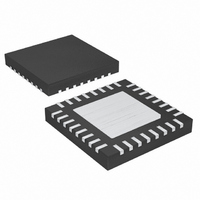
MAX4890ETJ+ Maxim Integrated Products, MAX4890ETJ+ Datasheet - Page 7

MAX4890ETJ+
Manufacturer Part Number
MAX4890ETJ+
Description
IC ETHERNET SWITCH OCTAL 32TQFN
Manufacturer
Maxim Integrated Products
Datasheet
1.MAX4890EETJ.pdf
(13 pages)
Specifications of MAX4890ETJ+
Function
Ethernet Switch
Circuit
8 x 2:1
On-state Resistance
5.5 Ohm
Voltage Supply Source
Single Supply
Voltage - Supply, Single/dual (±)
3 V ~ 3.6 V
Current - Supply
280µA
Operating Temperature
-40°C ~ 85°C
Mounting Type
Surface Mount
Package / Case
32-WFQFN Exposed Pad
Lead Free Status / RoHS Status
Lead free / RoHS Compliant
The MAX4890E/MAX4892E provide a single digital con-
trol SEL. SEL controls the switches as well as the LED
switches as shown in Table 1.
The on-resistance of the MAX4890E/MAX4892E is very
low and stable as the analog input signals are swept
from ground to V+ (see the Typical Operating
Characteristics). The switches are bidirectional, allow-
ing A_ and _B_ to be configured as either inputs or out-
puts.
The MAX4890E/MAX4892E are characterized using the
Human Body Model for ±15kV of ESD protection. Figure 5
shows the Human Body Model. This model consists of a
100pF capacitor charged to the ESD voltage of interest
which is then discharged into the test device through a
1.5kΩ resistor. All signal and control pins are ESD pro-
tected to ±15kV HBM (Human Body Model).
Table 1. Truth Table
1000 Base-T, ±15kV ESD Protection LAN Switches
SEL
0
1
_______________________________________________________________________________________
A_ to _B1, LED_ to _LED1
A_ to _B2, LED_ to _LED2
CONNECTION
Digital Control Inputs
Analog Signal Levels
ESD Protection
The Typical Operating Circuit shows the MAX4890E/
MAX4892E in a 1000 Base-T docking station application.
Caution: Do not exceed the absolute maximum ratings.
Stresses beyond the listed ratings may cause perma-
nent damage to the device.
Proper power-supply sequencing is recommended for
all CMOS devices. Always apply V+ before applying
analog signals, especially if the analog signal is not
current limited.
High-speed switches require proper layout and design
procedures for optimum performance. Keep design-con-
trolled-impedance pc board traces as short as possible.
Ensure that bypass capacitors are as close as possible
to the device. Use large ground planes where possible.
PROCESS: BiCMOS
Applications Information
Power-Supply Sequencing and
Typical Operating Circuit
Overvoltage Protection
Chip Information
Layout
7


