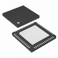
MAX4927ETN+ Maxim Integrated Products, MAX4927ETN+ Datasheet - Page 8

MAX4927ETN+
Manufacturer Part Number
MAX4927ETN+
Description
IC ETHERNET SWITCH QUAD 56TQFN
Manufacturer
Maxim Integrated Products
Datasheet
1.MAX4927ETN.pdf
(13 pages)
Specifications of MAX4927ETN+
Function
Ethernet Switch
Circuit
4 x 2:2
On-state Resistance
5.5 Ohm
Voltage Supply Source
Single Supply
Voltage - Supply, Single/dual (±)
3 V ~ 3.6 V
Current - Supply
280µA
Operating Temperature
-40°C ~ 85°C
Mounting Type
Surface Mount
Package / Case
56-TFQFN, Exposed Pad
Lead Free Status / RoHS Status
Lead free / RoHS Compliant
Figure 5a shows the Human Body Model. Figure 5b
shows the current waveform it generates when dis-
charged into a low impedance. This model consists of a
100pF capacitor charged to the ESD voltage of interest,
which is then discharged into the test device through
1.5kΩ resistor.
The IEC 61000-4-2 standard covers ESD testing and
performance of finished equipment. However, it does
not specifically refer to integrated circuits. The MAX4927
helps equipment design to meet IEC 61000-4-2 without
the need for additional ESD-protected components.
The major difference between tests done using the
Human Body Model and IEC 61000-4-2 is higher peak
current in IEC 61000-4-2 because series resistance is
lower in the IEC 61000-4-2 model. Hence, the ESD with-
stand voltage measured to IEC 61000-4-2 is generally
lower than that measured using the Human Body
Model. Figure 5c shows the IEC 61000-4-2 model, and
Figure 5d shows the current waveform for IEC 61000-4-
2 ESD Contact Discharge test.
The machine model for ESD tests all pins using a 200pF
storage capacitor and zero discharge resistance.
The objective is to emulate the stress caused when I/O
pins are contacted by handling equipment during test
and assembly.
The Air-Gap Discharge Method involves approaching the
device with a charged probe. The Contact Discharge
Method connects the probe to the device before the
probe is energized.
1000 Base-T, ±15kV ESD Protection LAN Switch
8
_______________________________________________________________________________________
Human Body Model
Machine Model
IEC 61000-4-2
The Typical Operating Circuit shows the MAX4927 in a
1000 Base-T docking station application.
Caution: Do not exceed the absolute maximum ratings.
Stresses beyond the listed ratings may cause perma-
nent damage to the device.
Proper power-supply sequencing is recommended for
all CMOS devices. Always apply V
analog signals, especially if the analog signal is not
current limited.
Bypass at least one V
larger ceramic capacitor as close to the device as pos-
sible. Use the smallest physical size possible for optimal
performance (0603 body size is recommended).
It is also recommended to bypass more than one V
input. A good strategy is to bypass one V
a 0.1µF capacitor, and at least a second V
a 10nF capacitor (use 0603 or smaller physical size
ceramic capacitor).
High-speed switches require proper layout and design
procedures for optimum performance. Keep design-con-
trolled-impedance PCB traces as short as possible.
Ensure that bypass capacitors are as close as possible
to the device. Use large ground planes where possible.
PROCESS: BiCMOS
Power-Supply Bypassing
Applications Information
Power-Supply Sequencing and
DD
Typical Operating Circuit
input to ground with a 0.1µF or
Overvoltage Protection
Chip Information
DD
before applying
DD
DD
input with
input with
Layout
DD


