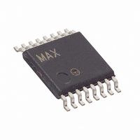
MAX4711EUE+ Maxim Integrated Products, MAX4711EUE+ Datasheet - Page 11

MAX4711EUE+
Manufacturer Part Number
MAX4711EUE+
Description
IC SWITCH QUAD SPST 16TSSOP
Manufacturer
Maxim Integrated Products
Datasheet
1.MAX4712ESE.pdf
(17 pages)
Specifications of MAX4711EUE+
Function
Switch
Circuit
4 x SPST - NC
On-state Resistance
25 Ohm
Voltage Supply Source
Single, Dual Supply
Voltage - Supply, Single/dual (±)
2.7 V ~ 11 V, ±2.7 V ~ 5.5 V
Operating Temperature
-40°C ~ 85°C
Mounting Type
Surface Mount
Package / Case
16-TSSOP
Lead Free Status / RoHS Status
Lead free / RoHS Compliant
Figure 1. Block Diagram
NC_) and COM_ so that signals pass equally well in
either direction.
When the signal on NO_ (or NC_) exceeds V+ by about
150mV, the high-fault comparator output is high, turn-
ing off FETs N1 and P1. This makes the NO_ (or NC_)
input high impedance regardless of the switch state. If
the switch state is “off”, all FETs are turned off and both
NO_ (or NC_) and COM_ are high impedance. If the
switch state is “on”, clamp FET P2 is turned on, sourc-
ing current from V+ to COM_.
When the signal on NO_ (or NC_) exceeds V- by about
150mV, the low-fault comparator output is high, turning
off FETs N1 and P1. This makes the NO_ (or NC_) input
high impedance regardless of the switch state. If the
switch state is “off”, all FETs are turned off and both
NO_ (or NC_) and COM_ are high impedance. If the
switch state is “on”, clamp FET N2 is turned on, sinking
current from COM_ to V-.
(NC_)
GND
NO_
IN_
V+
V-
-ESD DIODE
______________________________________________________________________________________
Negative Fault Condition
Positive Fault Condition
NC SWITCH
FAULT
FAULT
HIGH
LOW
ON
NORMALLY OPEN SWITCH CONSTRUCTION
Fault-Protected, Low-Voltage,
Quad SPST Analog Switches
When a fast rise-time or fall-time transient on NC_ or
NO_ exceeds V+ or V-, the output (COM_) follows the
input to the supply rail with only a few nanoseconds
delay. This delay is due to the switch on-resistance and
circuit capacitance to ground. When the input transient
returns to within the supply rails, however, there is a
700ns output recovery delay time. These values
depend on the COM_ output resistance and capaci-
tance, and are not production tested or guaranteed.
The delays are not dependent on the fault amplitude.
Higher COM_ output resistance and capacitance
increase recovery times.
FETs N2 and P2 can source about ±15mA from V+ or
V- to COM_ in the fault condition. Ensure that if the
COM_ pin is connected to a low-resistance load, the
absolute maximum current rating of 40mA is never
exceeded both in normal and fault conditions.
Transient Fault Response and Recovery
N1
P1
COM_ and IN_ Pins
P2
N2
COM_
11


